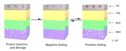
Using a quantum material called a correlated oxide, researchers at Harvard University (Cambridge, MA) have achieved a reversible change in electrical resistance of eight orders of magnitude, a result the researchers are calling "colossal."1 Because the correlated oxides can function equally well at room temperature or a few hundred degrees above it, it would be easy to integrate them into existing electronic devices and fabrication methods. The discovery, published in Nature Communications, therefore firmly establishes correlated oxides as promising semiconductors for transistors in future 3D integrated circuits as well as for adaptive, tunable photonic devices.
"By a certain choice of dopants—in this case, hydrogen or lithium—we can widen or narrow the band gap in this material, deterministically moving electrons in and out of their orbitals," says Shriram Ramanathan, associate professor of materials science at the Harvard School of Engineering and Applied Sciences (SEAS). This is a fundamentally different approach than is used in other semiconductors; the traditional method changes the energy level to meet the target, while the new method moves the target itself.
Unlike silicon, samarium nickelate and other correlated oxides are quantum materials, meaning that quantum-mechanical interactions have a dominant influence over the material properties—and not just at small scales.
"If you have two electrons in adjacent orbitals, and the orbitals are not completely filled, in a traditional material the electrons can move from one orbital to another. But in the correlated oxides, the electrons repulse each other so much that they cannot move," says Ramanathan. "The occupancy of the orbitals and the ability of electrons to move in the crystal are very closely tied together, or 'correlated.' Fundamentally, that's what dictates whether the material behaves as an insulator or a metal."
Ramanathan and others at SEAS have successfully manipulated the metal-insulator transition in vanadium oxide. In 2012, they demonstrated a tunable device that can absorb 99.75% of infrared light, appearing black to infrared cameras.
Similarly, samarium nickelate is likely to catch the attention of applied physicists developing photonic and optoelectronic devices.
"Opening and closing the band gap means you can now manipulate the ways in which electromagnetic radiation interacts with your material," says Jian Shi, lead author. "Just by applying an electric field, you’re dynamically controlling how light interacts with this material."
Source: http://www.seas.harvard.edu/news/2014/09/for-electronics-beyond-silicon-new-contender-emerges
REFERENCE:
1. Jian Shi et al., Nature Communications (2014); doi: 10.1038/ncomms5860

