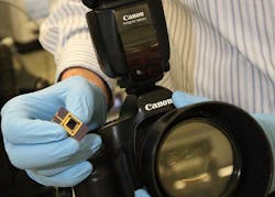
Albany, NY--Research by a team of State University of New York (SUNY) College of Nanoscale Science and Engineering (CNSE) scientists published in ACS Nano (see http://pubs.acs.org/doi/pdf/10.1021/nn405037s) describing the development of ultrathin "nanosheets" could make blurry nighttime pictures a thing of the past. The SUNY CNSE researchers say that the technology enables pictures to be captured in extremely low-light settings and could dramatically improve the performance of cell phone cameras, video cameras, medical imaging equipment such as MRI machines, and even solar cells.
The thin photodetectors would also be cost-effective to implement. The ultrathin indium (III) selenide (In2Se3)-based photodetectors use less material because they consist of nanosized components that are highly efficient at detecting light in real-time. As a result, this technology is perfectly suited for inclusion in a wide variety of everyday devices, including today's smartphones, which are often used to take pictures but still suffer from limitations such as an inability to take clear photos in low-light environments. This research could allow even novice photographers to be able to take sharper images in such dark situations, such as when a child is blowing out birthday candles in a dimly lit room.
"Currently, the sensors in digital cameras cannot take quality images under low-light conditions. For example, taking a good picture in a dimly lit room requires a long exposure which often results in a blurred image. Hollywood needs to use special lights and filters to make a scene appear dark because filming must be done in well-lit conditions. Future cameras based on these nanosheet photodetectors may be able to provide a robust, real-time picture in even the most extreme low-light conditions." said Robin Jacobs-Gedrim, CNSE Research Assistant. "Our work could also lead to next-generation applications, making solar panels more efficient, scientific instruments more precise, and medical imaging equipment even more accurate, which shows the power of CNSE's nano-based research to find technological solutions for a range of industries."
Bin Yu, CNSE professor of Nanoengineering, said, "This research is exciting not only because it is a further testament to the caliber of CNSE's scientists and state-of-the-art facilities, but also because it could lead to more efficient imaging devices for the improvement of healthcare, the advancement of real-time video recording, and the development of more efficient photovoltaics, all of which have the potential to improve countless lives."
CNSE (http://www.sunycnse.com) is a university-driven research enterprise, with more than $20 billion in high-tech investments and over 300 corporate partners. The 1.3 million-square-foot Albany NanoTech megaplex is home to more than 3100 scientists, researchers, engineers, students, and faculty. CNSE maintains a statewide footprint, operating the Smart Cities Technology Innovation Center (SCiTI) at Kiernan Plaza in Albany, the Solar Energy Development Center in Halfmoon, the Photovoltaic Manufacturing and Technology Development Facility in Rochester, and the Smart System Technology and Commercialization Center (STC) in Canandaigua. CNSE co-founded and manages the Computer Chip Commercialization Center (Quad-C) at SUNYIT, and is lead developer of the Marcy Nanocenter site in Utica, as well as the Riverbend Green Energy Hub, High-Tech Manufacturing Innovation Hub, and Medical Innovation and Commercialization Hub, all in Buffalo.
SOURCE: SUNY; http://www.sunycnse.com/leadingedgeresearchanddevelopment/researchprofiles.aspx

