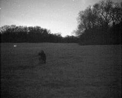
Within the near-infrared spectral region, an emerging class of detectors solve critical needs in both military and commercial markets, with applications ranging from harvesting photons in the night sky for digital night vision to next-generation gesture recognition technology and biometrics.
JAMES E. CAREY and MARTIN U. PRALLE
Image sensor innovation has centered on reducing the cost, size, weight and power of cameras and other image capture devices while increasing resolution and color fidelity to ensure the resulting imagery is a detailed, near-perfect rendition of the original scene. In particular, complementary metal-oxide semiconductor (CMOS) image sensors have proven highly effective in meeting this objective, with annual sales of more than two billion units, annual revenues exceeding $6 billion, and continued double-digit sales growth.1
However, CMOS image sensors are spectrally limited primarily to visible wavelengths because of silicon’s low native sensitivity to infrared (IR) light. As an indirect bandgap semiconductor material, silicon requires the combination of a photon and a phonon to absorb light and generate an electron-hole pair. As the wavelengths approach the band edge, the probability for absorption decreases, and the photons penetrate deeper into the silicon substrate.2 Most CMOS imagers are fabricated on physically thin layers (<5 μm) of optically active silicon material and exhibit a precipitous fall-off in sensitivity at wavelengths longer than 800 nm.
While the majority of the market for CMOS image sensors is driven by visible imaging, there is a rapidly growing market that requires low-cost, high-performance sensors capable of imaging in the near-infrared (NIR). Applications for NIR imaging are varied and range from low-cost night vision solutions in both military and homeland security applications to the consumer need for computational imagers in gesture recognition interfaces and biometric identification systems. By dramatically enhancing the NIR sensitivity of CMOS image sensors, SiOnyx has achieved a technological improvement for these applications and, critically, has done so without loss of performance in the visible color spectrum.
Extended quantum efficiency
A combination of ultralow noise image sensor design and our proprietary black silicon NIR enhanced sensing technology enables broad-spectral-response sensors operating from 400 to 1200 nm with approximately 2 e- of read noise within a monolithic CMOS solution. Extended quantum efficiency (trademarked XQE) SiOnyx sensors deliver increased IR quantum efficiency to enable as much as a 10X improvement (for wavelengths greater than 1000 nm) compared to incumbent CMOS solutions. This is a critical spectral region for night vision applications for which there are a significant number of “night-glow” photons emitted from molecules high up in the earth’s atmosphere.
Fabricated using a high-throughput, ultrafast laser process that has been optimized over the last decade, enhanced IR sensitivity is achieved on the same thin layer of silicon that is used in standard silicon CMOS image sensors. Because modern CMOS image sensors are some of the most electrically sensitive devices (e.g., recording noise characteristics in individual electrons), it is essential to maintain a pristine crystalline structure. Ultrafast laser processing satisfies this stringent requirement, since ultrafast laser interaction with the silicon substrate means essentially zero propagation of defects into the material.3 The optimized, proprietary ultrafast laser process does not cause an increase in dark current, read noise, or lag as compared with that of standard process control devices. This ability to significantly boost quantum efficiency (QE) while not degrading any other device parameters is a critical achievement.
Earlier this year, SiOnyx released its first black silicon enhanced image sensors for the night vision and surveillance markets with NIR sensitivity of 4X to 10X incumbent technologies (depending on the wavelength of interest). The SiOnyx XQE-1310 in particular delivered imaging at 60 Hz in a scene with 1 mlux illuminance—representative of a clear moonless night sky.4 The capability to image in conditions all the way from full noon sun to moonless starlight with a single focal plane array expands the market potential for both military and consumer applications.
Commercial markets
The commercial security and surveillance market is experiencing rapid growth, in large part from the increasing reliance on cameras to provide public safety and information to officials in urban environments. Similar to military markets, demanding surveillance situations require high-performance visible imaging and low-light imaging capability. The end user can take advantage of increased NIR sensitivity in a number of ways, including unassisted night imaging in light-starved outdoor locations, increasing the range and field of view for NIR-illuminated scenes, or the ability to reduce power and lighting requirements at the location under surveillance.
In addition to traditional imaging applications such as commercial security cameras, the last few years have witnessed many new products that use NIR light to provide methods of human/machine interaction. Computational imaging applications, including gesture recognition, eye tracking, time-of-flight, and automotive passenger monitoring, rely on IR light to avoid interfering with the way people visualize and interact with their environment. All of these applications benefit from increased sensitivity in the NIR and are only addressable by high-volume, inexpensive, and compact camera modules.
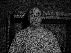
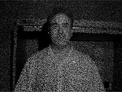
For gesture recognition applications, for example, a known structured-light pattern of 850 nm illumination such as a “point cloud” shines onto a scene and is imaged by a sensor that is placed at a known distance from the light source (see Fig. 1). Using geometric relationships such as triangulation, the image can be processed to create a three-dimensional map of the scene and track gestures made by the subject. Black silicon sensors provide up to double the QE and signal-to-noise ratio at 850 nm, which translates into better recognition of gestures or a reduction in the necessary light power.
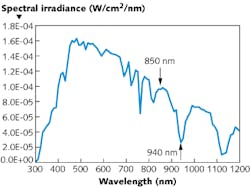
For mobile consumer electronics devices, it is critical that computational imaging algorithms work in widely varying ambient light environments. One particularly challenging environment is outdoor, daytime use since radiation from the sun tends to swamp out any controlled illumination required for the computational system. The majority of the technologies deployed today use 850 nm IR illumination because that wavelength simultaneously has low-cost illuminators available and still allows for at least some sensitivity in traditional CMOS image sensors. However, the sun’s spectrum contains a relatively high amount of power at 850 nm (see Fig. 2), and this background signal severely limits the performance of these computational systems. Fortunately, at wavelengths around 940 nm, the sun’s power is relatively low (due to absorption in the atmosphere) and inexpensive light sources are available. Since most CMOS image sensors have very poor QE at 940 nm, incumbent systems have so far been forced to operate at the inferior 850 nm node.
spectrum at the surface of the Earth.
The added sensitivity at 940 nm—more than 3X better than incumbent sensors—of XQE sensors coupled with lower background radiation at that wavelength allows the mobile hardware designer to conserve power through reducing the amount of illuminant needed for the measurement, increasing the distance at which their detection algorithms are effective, or capitalizing on the better signal-to-noise ratio to improve performance (see Fig. 3).
Military/homeland security markets
The military’s need to establish asymmetric warfighter advantage in nighttime operations has driven extensive developments in night vision technology. Incumbent image intensifier solutions use a very sensitive photomultiplier tube to amplify optical signals and display them on a phosphorescent screen. For the past 60 years, these devices have been iteratively improved upon and today they demonstrate outstanding performance down to overcast moonless starlight conditions. However, intensifier tubes are an analog technology that has fundamental limitations including significant blooming under bright illumination in the scene, manual gain control, and a complete lack of sensitivity to wavelengths beyond 910 nm—excluding laser designators at 1064 nm.5
A digital night vision solution with high NIR sensitivity can offer an alternative to image intensifier tubes by leveraging nightglow photons that are not available to intensifier tubes. As such, it is possible to achieve the required nighttime imaging performance while providing the benefits of a digital solution, such as remote transmission of imaging data or the ability to run extensive image processing
algorithms. Digital sensors deployed in distributed mobile units can wirelessly transmit information back to central command so that military commanders can best assess the situation to make real-time decisions accordingly. Likewise, centralized monitoring of perimeters and fixed assets is only possible with a digital solution.
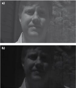
Outside of traditional low-light imaging applications, there is a very strong need for imaging systems that are also capable of “seeing” critical lasers. Known as “see-spot” imagers, these devices must easily image a laser signature within an operational scene, including the most commonly used target or designator wavelength of 1064 nm. The XQE image sensors provide more than a 10X increase in 1064 nm sensitivity over other CMOS image sensors and enable simultaneous low-light imaging of a scene and see-spot designator imaging in the same sensor (see Fig. 4). In addition, the high sensitivity of the sensors at 1064 nm allows for see-spot imaging in the extremely challenging environment of a brightly lit scene (such as daylight).
REFERENCES
1. See http://bit.ly/123ybFP.
2. S. M. Sze and K. K. Ng, Physics of Semiconductor Devices, John Wiley & Sons, New York, NY (1981).
3. S. K. Sundaram and E. Mazur, Nat. Mater., 1, 4, 217–224 (2002).
4. RCA Electro-Optics Handbook, Technical Series EOH-106, 6 (1968).
5. E. Bender, Electro-Optical Imaging: System Performance and Modelling, ch. 5., SPIE Press (2001).
James E. Carey is principal scientist and co-founder and Martin U. Pralle is VP of business development at SiOnyx, 100 Cummings Center 243F, Beverly, MA 01915; email: [email protected]; www.sionyx.com.
