Optically pumped strained Ge nanowire laser aims at CMOS-compatible photonic circuits
The holy grail for silicon (Si) photonics is to have all photonic-circuit components, both passive and active, able to be fabricated using standard CMOS techniques, without the need for hybrid active devices (for example, lasers and detectors at least partially made from III-V semiconductors such as aluminum gallium indium arsenide or others). Such a configuration is easy and cheap to mass-produce, and allows tight integration of electronics with photonics. The problem is that Si, along with the similarly CMOS-compatible group-IV semiconductor germanium (Ge), do not naturally emit light when pumped, as III-V semiconductors can—wringing light from Si or GE (or a combination of the two) requires exotic techniques that seem to never work out in practice.
One of these techniques, creating lasers out of highly strained Ge, has been pursued up until now without much success. However, a team of researchers from Nanyang Technological University (Singapore), Singapore-MIT Alliance for Research and Technology (Singapore), Inha University (Incheon, South Korea), and Stanford University (Stanford, CA) has unveiled a type of Ge laser made from highly tensile-strained nanowires that not only lases, but has a low lasing threshold of about 3.0 kW/cm2 at its output wavelength of 1510 nm. Although the device is optically pumped and operates at 83 K, it points the way toward room-temperature group-V CMOS-compatible lasers for optical integrated circuits.
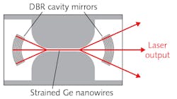
In the laser, the Ge nanowires are sandwiched by two stressing pads that place the nanowires under a 1.6% uniaxial tensile strain-the laser cavity is defined by two distributed Bragg reflectors (DBRs). Unlike other configurations in which the strained Ge has been suspended in air, this new geometry places the Ge against silicon dioxide (SiO2), which efficiently conducts heat away while still maintaining optical confinement in the Ge. The laser was pumped with intensities up to 14.6 kW/cm2, with a multimode output and with the full width at half maximum (FWHM) linewidth of a single cavity mode being about 1.3 nm, corresponding to a quality factor (Q) of more than 1100. Reference: S. Bao et al., arXiv:1708.04568v1 [physics.optics] (2017).
About the Author

John Wallace
Senior Technical Editor (1998-2022)
John Wallace was with Laser Focus World for nearly 25 years, retiring in late June 2022. He obtained a bachelor's degree in mechanical engineering and physics at Rutgers University and a master's in optical engineering at the University of Rochester. Before becoming an editor, John worked as an engineer at RCA, Exxon, Eastman Kodak, and GCA Corporation.