Laser-damage Testing: New laser-damage evaluation techniques boost testing capabilities

As laser technology has advanced to include higher laser powers, shorter pulses, and exotic wavelengths, the optical components that support these lasers, including cavity optics and beam-transport components, have been forced to evolve as well. With lasers operating from the femtosecond regime to continuous-wave (CW), optics manufacturers are now being asked to provide a multitude of solutions for a broad base of customers.
New evaporative processes and novel process control have helped advance the state of the art for optical coatings. However, one of the limiting mechanisms in the development of higher-power laser sources is the ability of these coatings to withstand power without exhibiting laser-induced damage or degradation.
Integral to process development and manufacturing is the ability to perform a well-defined and statistically relevant measurement on the damage threshold of optical components over a broad range of wavelengths and pulse formats. There is no one test that provides a panacea, so proper testing requires a multitude of lasers emulating the wavelengths, pulse formats, and pulse energies that the components will see in their eventual applications. There is, however, a general framework that should be implemented in designing and implementing a specific damage test procedure.
This article will discuss one of the most important concepts that must be understood to define a proper test procedure and to interpret its results. While a significant portion of this measurement technique has been embedded in the ISO-21254 laser-damage testing specification, we will discuss a novel and exciting test method that has furthered the ability to perform a relevant damage test, and is in the early stages of implementation towards a revised measurement standard.
As part of this discussion, we will be talking strictly about laser damage occurring in thin films. This technique, however, can be relevant for testing bulk optical properties of materials as well.
The defect-driven damage model
To understand certain mechanisms of laser damage and to help design a proper test that interrogates the film surface, one must make an assumption concerning the deposition process.
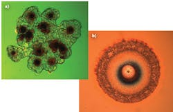
The basis behind the defect model is that any film deposited on a substrate will have defects that are intrinsic to the specific deposition process and the materials used in that process.1 It is important to understand that these defects can act as preferential damage precursors because of absorption, electric field perturbation, and in some cases microfocusing of the laser beam (see Fig. 1).2
Sometimes, these defects are easily observed using differential-interference contrast (DIC) microscopy or dark-field microscopy, or by imaging the scatter from the optical surface. In other cases, these defects cannot be observed with optical instrumentation because of their diminutive size or location within the film. These defects tend to be randomly distributed on the film and can be defined by a specific defect density. The nature of the defect is that the optical coating, driven by these defects, will have a damage threshold below the intrinsic damage threshold of the film.
Upon understanding this defect-driven damage mechanism, it becomes obvious that when performing a test, a sufficient area of the surface must be interrogated to provide a high confidence that the defects have been found and irradiated.3 For this reason, damage testing should be performed with as large a beam as possible.
Because of laser constraints, however, it is not always convenient to have a laser source that can test a sample with a laser beam diameter at the full clear aperture. It is also important to understand that when using a Gaussian beam to test a sample (currently accepted test protocol), the diameter or the "peak" region of that beam, as defined by the region where the beam energy drops by 10% of the central maximum, is nominally 18% of the beam diameter when defined at the 1/e2 point.
For example, a laser beam with a diameter of 1 mm defined by its 1/e2 points would have a peak-region diameter of nominally 180 μm. Certainly, 1 mm spots can be effectively used in certain high-energy laser systems (where even this beam size would be considered small). However, for CW or high-repetition-rate laser systems, or lasers with lower pulse energy, smaller spots must be used to increase fluence, reducing the effective area interrogated.
Raster-scanning technique
A method that has been implemented for interrogating larger test areas, therefore increasing the confidence that defects are being irradiated, is the emergence of a novel raster-scan technique. This technique was developed at Lawrence Livermore National Laboratory (Livermore, CA) in an effort to scale reduced test areas to damage characterization of large optics prior to the construction of NIF.4
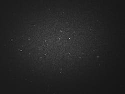
In this technique, individual laser pulses are indexed in a serpentine raster pattern in which individual pulses are separated, in distance, by the 90% point of the Gaussian peak for a chosen focused spot diameter. This 90% separation is used in both the x and y direction of the raster scan. The scan is conducted over a predefined portion of the optic under test, and the onset of damage is observed either using a scatterometer making a real-time measurement (see Fig. 2) or using inspection of the surface via microscope before and after irradiation. If a successful (no observed damage) raster scan has been completed at a specific level, the laser fluence is increased by a predetermined amount and the raster scan run again following this pattern until damage to the surface is observed.The advantage of this technique is that, essentially, when the footprints of the Gaussian beams are overlapped, the convolution of the overlapped beams provides a "bumpy" flat-top beam over the chosen scan area. The scan area can be any size up to the full aperture of the optic under test. If desired, the test can be designed, providing complete coverage of the clear aperture and therefore a 100% confidence level that all film defects have been interrogated.
Specific variants of the test procedure can be performed, depending on the requirements for the test and the desired result. In applications where the test area is a large percentage of the clear aperture, the raster test is performed over the same area over and over. This provides a measurement known as a "conditioned" test, or R:1, where energy is ramped in the same area. If a smaller scan area is used and the clear aperture is larger, a fresh site can be utilized for each fluence level, providing a 1:1 or S:1 test where each location is irradiated with a single pulse or multiple pulses on a single site.
In conclusion, this raster-scan method provides a useful alternative to the standard ISO-21254. Further refinement of this test procedure will allow the user to design a test that includes a specific confidence level of the measurement at the chosen fluence for the specific end user.5
REFERENCES
1. C. J. Stolz et al., "Electric-field enhancement by nodular defects in multilayer coatings irradiated at normal and 45° incidence," Proc. SPIE, 5273, 41 (Jun. 10, 2004).
2. J. Wang, "Laser induced damage threshold prediction of dielectric enhanced mirrors at 1064 nm," Proc. SPIE, 9453, 94530S (May 22, 2015).
3. J. W. Arenberg and M. D. Thomas, Opt. Eng., 53, 12 (2014).
4. M. J. Runkel and M. C. Nostrand, "Overview of raster scanning for ICF-class laser optics," Proc. SPIE, 4932, 136 (May 28, 2003).
5. J. W. Arenberg et al., "Periodic review of ISO 21254: U.S. National Committee proposal for revision," Proc. SPIE, 10014, 10014-25 (2016).
About the Author
Michael Thomas
President, Spica Technologies
Michael Thomas is president of Spica Technologies (Hollis, NH), and also chairs a committee under the Optics and Electro-Optics Standards Council (OEOSC) tasked to generate a new U.S. laser-damage standard for the measurement of laser damage on optical components.
