CMOS Cameras: Back-illuminated sCMOS technology boosts low-light imaging and spectroscopy applications
For more than five decades, cameras that utilize silicon-based charge-coupled devices (CCDs) and their more recent variants—electron-multiplying CCDs (EMCCDs) and intensified CCDs (ICCDs)—have enabled numerous scientific discoveries. These versatile detectors are employed on a daily basis worldwide in physical and life science applications as diverse as single-molecule fluorescence, quantum imaging, astronomy, and spectroscopy.
Over the past several years, scientific complementary metal-oxide semiconductor (sCMOS) cameras capable of achieving low read noise and higher frame rates have begun to gain a degree of popularity as an alternative to CCD cameras for certain applications. However, the first generations of these sCMOS devices fell short on sensitivity because of their front-illuminated architecture, which imposes a fundamental limit on quantum efficiency (i.e., the fraction of incident photons detected in each pixel).
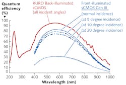
Aided by the latest CMOS fabrication technology, it is now possible to create sCMOS devices that implement a back-illuminated sensor architecture. As a result, these sensors are now capable of providing CCD-like quantum efficiency (>95% peak) and dynamic range without compromising the low read noise and higher frame rates for which sCMOS sensors are known.
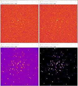
Back-illuminated sCMOS camera technology is a serious contender as an optical detector for many applications, including hyperspectral imaging, astronomy (see Fig. 1), cold-atom imaging, quantum imaging, fluorescence spectroscopy, and high-speed spectroscopy. This article discusses the key features and performance characteristics of the new technology, and compares it to other low-light detection technologies.
Back-illuminated architecture
With their higher sensitivity over a broader spectral region (deep-UV to near-IR), back-illuminated detectors are preferred over front-illuminated detectors for ultra-low-light applications such as astronomy, Raman spectroscopy, and biological imaging. The difference between front- and back-illuminated sensors is apparent at a glance. Front-illuminated sensors are reflective in appearance because most of the incident light is reflected back to the viewer, whereas back-illuminated sensors are visibly darker, owing to their absorption of most of the incident light.
Since front-illuminated sCMOS sensors contain readout/conversion circuitry inside every pixel, only a portion of each pixel is sensitive to light. This portion is referred to as the "fill factor" of the pixel. Most front-illuminated sCMOS sensors have microlenses on top of each pixel to refocus the incoming light into the photosensitive part of the pixel and increase the effective fill factor. Although microlenses help improve the light-collection efficiency of a front-illuminated sensor, they also carry certain drawbacks that limit the performance of most of these sCMOS cameras.Even though the layout of microlenses has been improved by various CMOS manufacturers, the angular dependency of photoresponse causes non-uniformity, especially at the edges of the sensor. In addition, these microlenses are typically made of plastic-like materials that transmit very poorly, or not at all, in the UV region (below 400 nm). The lack of microlenses in a back-illuminated sCMOS sensor's architecture translates to outstanding response in the UV range.
Frame rates and read noise
The latest generation of cameras based on back-illuminated sCMOS sensors offers very high frame rates. For example, KURO cameras from Princeton Instruments can provide up to 82 frames/s at full 1200 × 1200 resolution and >3000 frames/s at reduced resolution.
With large full-well capacity and very low read noise, typically 1.5 e- rms, these cameras are capable of delivering true 16-bit dynamic range. And although sCMOS devices typically do not support on-chip binning, their ability to perform off-chip software binning after frame acquisition is often useful for spectroscopy applications.
Rolling and global shutter modes
An important feature of sCMOS sensors is the availability of rolling electronic shutter mode. This is distinct from global shutter or snapshot mode, which exposes all pixels at the same time. Global shutter is preferred when the object needs to be frozen in time. However, this mode typically causes the read noise to increase by as much as 1.5-2X compared to rolling shutter mode while decreasing the frame rate by 2X.
In rolling shutter mode, the first row of the sensor is exposed first, the second row is exposed after one line read time, and so forth. In other words, the last row of the sensor is exposed at "(N-1) × line time" after the first row. This may cause image artifacts when looking at high-speed events that occur significantly faster than the frame rate, but most scientific applications can work with rolling shutter mode as long as the frame rate is sufficiently high. Global shutter mode, on the other hand, is preferred for industrial imaging applications in which the objects under inspection are moving at a rapid pace.
Advanced camera designs offer a way to trigger external light sources/shutters so as to create a pseudo-global shutter mode. To do so, the camera simply outputs a TTL signal that goes high when all the pixels are exposing. This will, in effect, cause the pixels to take a snapshot of the event when it is illuminated.
Detector recommendations
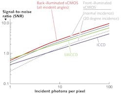
Scientists and engineers should carefully consider which sensor technology is best suited to their application. For example, signal-to-noise ratio (SNR) can be used to compare various technologies vs. incident number of photons per pixel (see Fig. 4). For each detector, peak quantum efficiency is assumed.While SNR is an important measure, other aspects of detector attributes must be considered before selecting a suitable detector. In general, for imaging or spectroscopy applications that require extended integration times (seconds to hours), CCD or EMCCD cameras are still preferred. This is also true for spectroscopy applications that require true on-chip binning. For time-resolved applications that require ultrafast gating (<500 ps to microseconds), intensified cameras (ICCD or emICCD) are the best choice. Back-illuminated sCMOS cameras provide the sensitivity and frame rates needed for all other applications with relatively short integration times (<10 s).
The table summarizes several important features of these sensor technologies and offers some general recommendations for different applications.
About the Author

Ravi Guntupalli
Product Manager
Ravi Guntupalli is a product manager at Princeton Instruments, a leading provider of scientific grade CCD, ICCD, EMCCD and InGaAs based cameras and spectrographs for ultra low light imaging and spectroscopy applications. With over 14 years of experience in the field of low light imaging technonologies, Ravi has been working with researchers worldwide who are applying these technologies across life and physical sciences.


