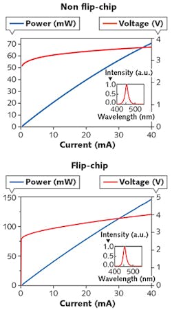
Flip-chip GaN-based LED has 73% wall-plug efficiency

Years of research have gone into enabling blue-emitting gallium nitride (GaN)-based LEDs, which are the basis for the white-light LEDs used widely for lighting, to produce more lumens per watt and, similarly, have a higher wall-plug efficiency (optical output in watts per electrical input in watts). Because p-GaN, a material used to make efficient GaN-based LEDs, has poor electrical conductivity and results in current-spreading, transparent conducting-oxide LEDs and flip-chip LEDs with silver mirrors have been developed as added conductors. However, the silver mirror or conducting oxide absorbs light, reducing overall efficiency.
A group at the University of California, Santa Barbara that includes Shuji Nakamura, one of the inventors of the GaN-based LED, is incorporating high-quality, low-voltage-drop GaN tunnel junctions into GaN-based LEDs, rather than conducting mirrors or oxides, to prevent current-spreading without adding to optical absorption. The researchers have created non-flip-chip and flip-chip versions, with the latter incorporating a high-light-extraction multilayer dielectric mirror that increased the reflectivity of the wire-bond pads to greater than 98% at the LED's 450 nm operating wavelength. The resulting external quantum efficiency (EQE) and wall-plug efficiency (WPE) of the non-flip-chip device were 78% and 72%, respectively, and for the flip-chip LED were 76% and 73%, respectively. Patents are pending on both the tunnel-junction and light-extraction technologies developed by the researchers. Reference: B. P. Yonkee et al., Appl. Phys. Lett., 109, 191104 (2016).
About the Author
John Wallace
Senior Technical Editor (1998-2022)
John Wallace was with Laser Focus World for nearly 25 years, retiring in late June 2022. He obtained a bachelor's degree in mechanical engineering and physics at Rutgers University and a master's in optical engineering at the University of Rochester. Before becoming an editor, John worked as an engineer at RCA, Exxon, Eastman Kodak, and GCA Corporation.
