Strong laser fields replace photoemission spectroscopy for band structure measurements
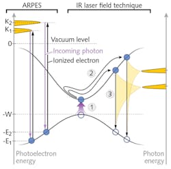
The "band structure" of a solid, or more simply the energy of electrons within the solid that controls its fundamental material properties such as conductivity, transparency, and even exotic states of matter such as superconductivity, is historically measured using angle-resolved photoemission spectroscopy (ARPES). Unfortunately, ARPES—wherein high-energy ultraviolet or x-rays bombard a solid, kicking out electrons that are then studied to reveal band structure—requires vacuum conditions that prevent measurement of ambient states of solids and can only see a thin layer of material, as deeper electrons remain buried.
Alternatively, a new technique from the University of Ottawa (Ottawa, ON, Canada) studies the high-energy photons created through high-harmonic generation within a solid that is illuminated with intense, low-energy infrared (IR) laser beams. These IR beams generate electrons and holes, and are set on a collisional path. The addition of a dimmer, higher-frequency optical laser field perturbs the path and induces a spectral signature on the high-harmonic light emitted upon collision. This signature is then used to dictate what band structure produced the result. Unlike ARPES, this IR laser field technique can study bulk solids, materials in high magnetic fields, and potentially even materials enclosed in highly pressurized diamond-anvil cells. Reference: G. Vampa, SPIE Newsroom (Aug. 31, 2016); doi:10.1117/2.1201608.006643.
About the Author

Gail Overton
Senior Editor (2004-2020)
Gail has more than 30 years of engineering, marketing, product management, and editorial experience in the photonics and optical communications industry. Before joining the staff at Laser Focus World in 2004, she held many product management and product marketing roles in the fiber-optics industry, most notably at Hughes (El Segundo, CA), GTE Labs (Waltham, MA), Corning (Corning, NY), Photon Kinetics (Beaverton, OR), and Newport Corporation (Irvine, CA). During her marketing career, Gail published articles in WDM Solutions and Sensors magazine and traveled internationally to conduct product and sales training. Gail received her BS degree in physics, with an emphasis in optics, from San Diego State University in San Diego, CA in May 1986.