Wearable Photonics: 1-μm-thick GaAs photovoltaic cells have a 1.4 mm bending radius
Because flexible photonic devices tend to contain optical detectors and/or emitters, they often have semiconductor materials in their configuration—but most bulk semiconductor materials are quite brittle. While one approach relies on many small discrete rigid semiconductor devices connected in a flexible wire grid or other conducting backplane, this results in an array of components that are like small, hard pebbles.
A second approach consists of thinning the material until it becomes flexible. If it is organic, that imparts an additional intrinsic flexibility. However, inorganic semiconductors often have qualities such as higher efficiency or better spectral characteristics—thinning them is the primary approach to making them flexible. And the thinner they're made, the more flexible they become.
Micrometer-scale thinness
Now, scientists from the Gwangju Institute of Science and Technology, the Korea Photonics Technology Institute, and Yeungnam University (all in South Korea) have made ultrathin 1-μm-thick gallium arsenide (GaAs) photovoltaic cells flexible enough to wrap around a pencil—such solar cells could power wearable electronics like fitness trackers.1 Standard photovoltaics are usually hundreds of times thicker than these solar cells, and even most other thin photovoltaics are 2–4 times thicker.
The GaAs cells consist of a large array of microcells, each cell on the order of 700 μm2 and with a vertical structure. The researchers transfer-printed the GaAs cells directly onto metal electrodes on a flexible substrate without using an interlayer adhesive that would add to the material's thickness. The transfer-printing process produced a yield of close to 100%. The cells were then cold-welded to the electrode on the substrate by applying pressure at 170°C and melting a top layer of photoresist that acted as a temporary adhesive. The photoresist was later peeled away, leaving the direct metal-to-metal bond. The microcells were encapsulated with a 2-μm-thick layer of epoxy.
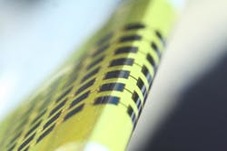
The researchers tested the efficiency of the devices at converting sunlight to electricity and found that the results (efficiencies from 14% to 15.2%) were comparable to those for similar thicker photovoltaics. One reason they were so efficient was that the metal bottom layer served as a reflector to recycle stray photons back to the solar cells. Bending tests showed that the 1.04-μm-thick cells could be wrapped around a radius as small as 1.4 mm, or even around a 1-mm-thick glass slide (see figure).
The team also performed a numerical analysis of the cells, finding that they experience one-fourth the amount of strain of similar cells that are 3.5 μm thick. "The thinner cells are less fragile under bending, but perform similarly or even slightly better," says Jongho Lee, one of the researchers. The single microcells have an open-circuit voltage of 0.99 V, and can be connected in series using sputtered metal lines (20 nm of chromium and 300 nm of gold) to produce an open-circuit voltage of, for example, 6.8 V for seven cells in series. Cycles of bending and unbending of up to 1000 times produce no degradation of the cells' efficiency or other properties.
A few other groups have reported solar cells with thicknesses of around 1 μm, but have produced the cells in different ways—for example, by removing the whole substrate by etching. By transfer printing instead of etching, the new method may be used to make very flexible photovoltaics with a smaller amount of materials. The thin cells can be integrated onto glasses frames or fabric, and might power the next wave of wearable electronics, Lee notes.
REFERENCE
1. J. Kim et al., Appl. Phys. Lett. (2016); doi:10.1063/1.4954039.
About the Author
John Wallace
Senior Technical Editor (1998-2022)
John Wallace was with Laser Focus World for nearly 25 years, retiring in late June 2022. He obtained a bachelor's degree in mechanical engineering and physics at Rutgers University and a master's in optical engineering at the University of Rochester. Before becoming an editor, John worked as an engineer at RCA, Exxon, Eastman Kodak, and GCA Corporation.

