CMOS Cameras: CAOS-CMOS camera has 1000X better dynamic range

Nabeel A. Riza, head of the School of Engineering and chair professor of Electrical and Electronic Engineering (EEE) at University College Cork (UCC; Cork, Ireland), and colleagues have demonstrated the coded access optical sensor (CAOS) complementary metal-oxide semiconductor (CMOS), or CAOS-CMOS, camera with a three-orders-of-magnitude (or factor of 1000) improvement in camera dynamic range when compared to a conventional CMOS camera.1 Using extremely bright and high-contrast test targets, it was demonstrated that the potentially high-speed camera has exceptionally low interpixel crosstalk and—using silicon-based photodetection—can operate from the ultraviolet (UV) to the near-infrared (near-IR) wavelength region.
High-contrast imaging
Major manufacturers have previously demonstrated CMOS multipixel sensor research devices with 80 dB dynamic range using a variety of techniques, including pixel-level light integration time and electronic gain controls, as well as by doubling sensor chip pixel size for larger quantum wells in rolling-shutter designs. However, imagers that function well beyond 80 dB are needed—especially for high-contrast (greater than 104:1) imaging applications such as welding, laser-beam profiling, combustion events, night vision, biological microscopy, and machine vision.
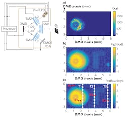
The CAOS-CMOS camera design uses electronic and optical pixel manipulation in both the space and time/frequency domain to form agile pixels that selectively act on CMOS sensor-guided regions of the image to observe unseen high-contrast features.
Light from an external object is directed by a lens (L1) onto the agile pixels plane of a programmable digital micromirror device (DMD). To initiate the imaging operation, the DMD micromirrors are set to spatially route the incident light to the CMOS sensor to create an initial target-scene irradiance map. Based on this initial image intelligence, the DMD is programmed in its CAOS mode to create specifically located agile pixels that sample image zones of interest.
This agile-pixel programming capability via the DMD allows the agile pixels to operate with different time-frequency coding methods such as frequency/code/time division multiple access (FDMA/CDMA/TDMA) schemes common in cell-phone radio-frequency (RF) communications. In addition, the point photodiode (PD) can be replaced by an avalanche PD, bolometer, or photomultiplier tube (PMT) point detector, while the CMOS sensor arm can also use a charge-coupled device (CCD) or focal-plane array (FPA) multipixel sensor type to enable different imaging applications across a diverse range of optical wavelengths.
All arms in the camera have an optional smart module (SM) that contains programmable optical conditioning elements such as variable apertures, on/off shutters, focus lenses, spectral filters, polarizers, and variable attenuators that can improve imaging performance, such as reducing saturation of the photodiode and CMOS sensor through electronic post-processing.
High dynamic range
By using the CAOS mode of the imager to view a test scene with extremely bright and dim image sections, experiments confirm that extraction of both the low- and high-intensity regions of the image can be accomplished to reconstruct a high-contrast image that was otherwise partly unseen when using the CMOS sensor alone. Experiments demonstrate a CAOS-CMOS camera dynamic range of 82.06 dB, which can be improved upon by further optimization of the camera hardware and image processing.
"The CAOS camera platform, when used in unison with current multipixel sensor camera technology, is envisioned to enable users to make a smart extreme-dynamic-range camera, opening up a world of the yet unseen," says Nabeel Riza.
REFERENCE
1. N. A. Riza et al., Opt. Express, 24, 12, 13444–13458 (2016).
About the Author

Gail Overton
Senior Editor (2004-2020)
Gail has more than 30 years of engineering, marketing, product management, and editorial experience in the photonics and optical communications industry. Before joining the staff at Laser Focus World in 2004, she held many product management and product marketing roles in the fiber-optics industry, most notably at Hughes (El Segundo, CA), GTE Labs (Waltham, MA), Corning (Corning, NY), Photon Kinetics (Beaverton, OR), and Newport Corporation (Irvine, CA). During her marketing career, Gail published articles in WDM Solutions and Sensors magazine and traveled internationally to conduct product and sales training. Gail received her BS degree in physics, with an emphasis in optics, from San Diego State University in San Diego, CA in May 1986.