Quantum Entanglement: Laser-machined actuator strains QDs to emit tunable entangled photons
Semiconductor quantum dots (QDs) are capable of generating indistinguishable polarization-entangled photons—however, methods to control the energy of the entangled photons have remained elusive until now. Researchers from Johannes Kepler University Linz (Linz, Austria), Forschungszentrum Mikrotechnik (Dornbirn, Austria), the Institute for Integrative Nanosciences, IFW (Dresden, Germany), and the Paul-Drude-Institut für Festkörperelektronik (Berlin, Germany) have developed a femtosecond-laser-machined piezoceramic actuator that provides three-directional strain engineering to tune the energy of entangled photons emitted by QDs without degrading the degree of entanglement of the photon pairs.1,2
A femtosecond-laser-structured actuator
The device processing begins by first fabricating the QD-embedded structure to be strained. Indium gallium arsenide (InGaAs)-based QDs grown at 500°C by molecular-beam epitaxy are embedded into a 300-nm-thick GaAs layer grown on top of a 100-nm-thick Al0.75Ga0.25As sacrificial layer. The sample is then coated with a 100-nm-thick chromium/gold (Cr/Au) layer and, in an epoxy photoresist process, is integrated via a flip-chip process onto a Cr/Au-coated, micromachined [Pb(Mg1/3Nb2/3)O3]0.72-[PbTiO3]0.28 (PMN-PT) piezo actuator. Finally, wet chemical etching is used to remove the Al0.75Ga0.25As sacrificial layer, thus leaving the 300-nm-thick QD-nanomembrane tightly bound to the piezoelectric actuator. The density is about 2 QDs/cm2.
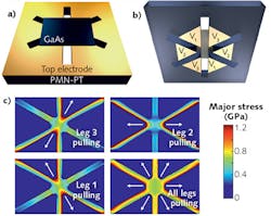
A 520 nm Spectra-Physics (Santa Clara, CA) Spirit femtosecond laser with 350 fs pulse duration, 25 kHz repetition rate, and an approximate 5 μm spot size was used to laser-structure the actuator substrate into a six-leg design (see figure). Six metal contacts were machined at the bottom of the piezo legs such that independent voltages could be applied with respect to the top ground contact.
Applying voltage to each pair of the actuator legs provides controlled deformation of the nanomembrane suspended at the central part of the actuator. That is, voltage applied to each pair of aligned legs creates an out-of-plane electric field that leads to an in-plane contraction or expansion of the piezo leg, thus transferring an in-plane tensile or compressive strain to the central part of the nanomembrane.
Tuning entanglement
Using the actuator to manipulate the strain of the QDs and their surrounding semiconductor matrix, the researchers demonstrated that it is possible to control the anisotropic electron-hole exchange interaction of QDs so as to modify "on-demand" the energy levels involved in the generation of entangled photons.
Collectively, they confirmed that the level of entanglement of their tunable photons—among the highest ever reported for QDs (fidelity to the expected entangled state as high as 0.82)—is not dependent on the photon energy. Furthermore, they demonstrated slow-entangled photons by using the strain actuator to interface the QDs with clouds of Cesium atoms.
While controllable energy is a fundamental requirement to interface the different nodes of a quantum network based on QDs, this controlled or "tuned" energy will be also critical for efficient photon storage of entangled photons in quantum memories based on atomic clouds or Bose-Einstein condensates.
Assistant professor Rinaldo Trotta at Johannes Kepler University Linz says, "These results represent not only a fundamental step towards the realization of solid-state-based quantum networks for the distribution of entanglement among distant parties, but the capability of our micromachined strain actuator of inducing widely variable in-plane strains—in anisotropy, direction, and magnitude—is expected to impact significantly the whole research area of strain engineering of semiconductor thin films."
REFERENCES
1. R. Trotta et al., Nature Commun., 7, 10375 (Jan. 27, 2016).
2. Patent WO 2015081361 A1 by Rastelli, Daruka, and Trotta.
About the Author

Gail Overton
Senior Editor (2004-2020)
Gail has more than 30 years of engineering, marketing, product management, and editorial experience in the photonics and optical communications industry. Before joining the staff at Laser Focus World in 2004, she held many product management and product marketing roles in the fiber-optics industry, most notably at Hughes (El Segundo, CA), GTE Labs (Waltham, MA), Corning (Corning, NY), Photon Kinetics (Beaverton, OR), and Newport Corporation (Irvine, CA). During her marketing career, Gail published articles in WDM Solutions and Sensors magazine and traveled internationally to conduct product and sales training. Gail received her BS degree in physics, with an emphasis in optics, from San Diego State University in San Diego, CA in May 1986.
