Technology Review: Top 20 technology picks for 2015 showcase wide scope of photonics advances
As in past years, this year's set of 20 top technology picks highlights the creativity and skill of the many scientists, engineers, technicians, and students—and, yes, managers and directors, too—who continue to drive the field of photonics forward at its breakneck pace. Possibly no other field can boast that it thrives on contributions from experts in optics, physics, mechanics, materials sciences, electronics, and chemistry (have I missed any?). In addition, no other field is blessed with highly skilled opticians, CAD designers, lab techs, and other adept people who advance the store of experience-based knowledge that is the foundation of photonics. You all have made possible not just this year's Tech Review Top 20 list, but the entire range of interconnected technologies that we call photonics.
1. Laser pixel for color displays.
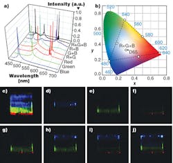
How might one very small bit of semiconducting material produce laser light of any color desired, including white? The question is a practical one, as an answer could lead to bright and efficient pixels for color displays. One solution, as determined by researchers at Arizona State University (Tempe, AZ) and Tsinghua University (Beijing, China), is to make the single pixel with a material composition that varies across the pixel, allowing it to be pumped—at single or multiple points—to produce different colors (see Fig. 1). The resulting chip, only 28.0 × 18.0 × 0.3 μm in size, is composed of zinc cadmium sulfide selenide (ZnCdSSe) in which the mix of Zn, Cd, S, and Se varies as a function of location. While the prototype is optically pumped, the researchers aim to soon produce an electrically pumped version. (See "Multicolor Lasers: Semiconductor laser can produce many colors, including white," LFW, September 2015; http://bit.ly/1Pn0gmH.)2. Lidar for everyone.
While one way to sense the position of objects in a 3D scene is to imitate human stereo vision by fusing information from two cameras to produce distance info, why not take a more straightforward approach and measure the distances directly using a laser beam? This, of course, is what light detection and ranging (lidar) systems do. Just one of the many advantages of lidar is that it can be made very small (in contrast, stereo 3D systems lose their distance-sensing ability when made small). However, for uses such as in autonomous vehicles, either the lidar light source must be very powerful, the photodetectors must be highly sensitive, or both. Fortunately, this technology is emerging, and resulting in small lidar systems that are already used in self-driving cars and can even be carried by small drones intended for infrastructure monitoring, disaster relief, and general surveillance. (See "LIDAR nears ubiquity as miniature systems proliferate," LFW, October 2015; http://bit.ly/1WwAimA.)
3. 3D printing of live cells.
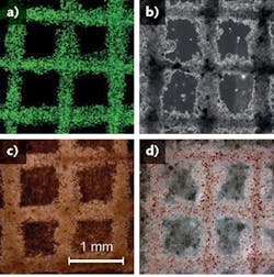
The rise of 3D printing (laser-based and otherwise) over the past few years allows the layer-by-layer fabrication of everything from aircraft parts to fine chocolates. Now, a laser-based forward-transfer method developed at Laser Zentrum Hannover (Hannover, Germany) enables 3D printing of live human cells, first for testing purposes and ultimately for construction of implantable organs (see Fig. 2). A glass slide or ribbon is coated first with a light-absorbing material and second with a layer of living cells in a gel. Focused pulses of 1064 nm laser light vaporize the absorber and impel a droplet of cells onto the desired surface, allowing both 2D and 3D patterns and objects to be printed. Experimenting with human skin cells, the researchers showed that the resulting structures, when implanted in mice, acquired blood vessels and showed differentiation of cells. (See "3D laser printing of live human cells promising for testing, transplantation," LFW, June 2015; http://bit.ly/1LQhA0Z.)4. Perfect resonator via moving plates.
Zubin Jacob of the University of Alberta (Edmonton, AB, Canada) describes how, in theory at least, certain limitations that apply to a conventional optical Fabry-Perot resonator can be overcome if the resonator's two plates are made to move with respect to one another. In fact, if the relative motion is fast enough, a perfect balance of both phase and amplitude can result, producing a potential infinitely high-quality (Q) factor. There are a few of hurdles to overcome, though: first, the gap between the plates must be held to about 10 nm, and second, the relative motion of the plates must reach on the order of one hundredth of the speed of light. Clearly, the second hurdle is a high one, which is why Jacob and his team are working on alternate approaches using sound waves and water waves to observe this resonance. The third hurdle is also big: a frictional force mediated by vacuum theoretically produces a large viscosity as the singular resonance is approached. Perhaps these effects can be at least partially achieved in the lab. (See "Moving photonics cause singular Fabry-Perot resonance," LFW, January 2015; http://bit.ly/1Spbh6S.)
5. EUV aims to give Moore's law another push.
What technological revolutions have occurred in the past 40 years or so? If you think about it, back in the 1970s humans already had left footprints on the moon and were exceeding the speed limit on interstate highways, crossing the Atlantic Ocean in supersonic aircraft, experimenting with artificial hearts, and nuking leftovers in their microwave ovens. The biggest change between then and now is the digital revolution and the technology it has inspired-all made possible by the development of ever-more-sophisticated computer chips. Right now, leading-edge computer chips have a 14 nm feature size, and silicon-based chip technology is limited to feature sizes of a few nanometers and above. Aiming at that small window left for silicon is extreme-ultraviolet (EUV) lithography. IBM Research (Albany, NY) has produced the first 7-nm-node test chips with functioning transistors, combining silicon with germanium to form the transistors. ASML (Veldhoven, Netherlands) is aiming at the 7 nm node by developing an EUV lithographic scanner. (See "Using EUV lithography, IBM research alliance produces first 7-nm-node test chips," LFW online, July 9th; http://bit.ly/1Spbt6g.)
6. Secure interferometric space communications.
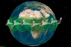
Satellite-to-satellite communications can provide the base for space-based wide-area networks, including server-to-server and router-to-router applications, with one caveat—the communications must be secure. While quantum cryptography, which is based on quantum entanglement of photons and necessitates the sensing of single photons, can serve as the path to security, another path exists: that of interferometric optical communications, which is based on large populations of indistinguishable photons. F. J. Duarte of Interferometric Optics (Rochester, NY) and Travis Taylor of the U.S. Army Space and Missile Defense Command (Huntsville, AL) propose a secure interferometric space communications system that could provide a simpler, smaller, and less-expensive alternative to secure satellite-to-satellite communications (see frontis). Based on a simple N-slit laser interferometer, the system does not need to count photons and can rely on room-temperature CCD or CMOS detectors. (See "Interferometry: Quantum entanglement physics secures space-to-space interferometric communications," LFW, April 2015; http://bit.ly/1iDqR1Z.)
7. Supernarrow-linewidth frequency conversion with short crystals.
Wavelengths of coherent light that are difficult to produce with lasers are commonly generated using frequency conversion of light by nonlinear optical crystals. However, the narrower the linewidth desired, the longer the crystal has to be made to create it—some applications such as communications that require ultranarrow linewidths can require crystals of unwieldy length. Roei Remez and Ady Arie of Tel Aviv University (Tel Aviv, Israel) have come up with a way around this problem by developing a superoscillatory nonlinear crystal that they compared to a conventional periodically poled crystal. Rather than a single section, the superoscillatory device has three periodically poled sections with differing duty cycles. The experimental superoscillation spectral bandwidth of 1.1 nm was 69% narrower than the 3.6 nm width of the central lobe in the conventional crystal of the same overall length. (See "Nonlinear crystal does supernarrow-linewidth frequency conversion," LFW, June 2015; http://bit.ly/1QdplkO.)
8. Intraocular lens focuses like a real eye.
The holy grail of corrective lenses for people with nonideal eyesight is the creation of a lens that can focus itself. While autofocusing eyeglasses have been developed, they are heavier than ordinary glasses and pick a focus based on their own sensors, which may not coincide with what the wearer wants. Now, engineers at biolnic (Cologne, Germany) have developed a flexible intraocular lens that is fully controlled by the human eye's own ciliary muscle. The result is naturally functioning vision that has an accommodation of 3 diopters around the relaxed focal position, allowing both near and far vision. The lens, called the DeepSight, has a high-refractive-index polymer shell and a liquid core and is implanted via the same medical procedure used for conventional intraocular lenses. (See "Bio-inspired intraocular lens mimics natural, adjustable vision," LFW, March 2015; http://bit.ly/1SpbQ0F.)
9. Nanoscale coherent imaging.
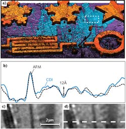
Microscopy techniques with subdiffraction-limited resolution, such as stimulated-emission-depletion (STED) and others, have opened up a new region of nanometer-scale imaging. However, along with the fact that they require extensive sample preparation, they cannot image the functioning of 3D nanosystems. Scientists at JILA/University of Colorado Boulder and KMLabs (Boulder, CO) have added high-harmonic generation (HHG) to coherent diffraction imaging (CDI) to create a system that imaged a test pattern with 22 nm resolution. The HHG provides short-wavelength extreme-ultraviolet (EUV) light, while CDI is a lensless technique that is suitable for use with EUV. In addition to high lateral resolution, CDI is a threefold combination of absorption- and geometric/material-dependent phase shifts that can produce images with subnanometer axial resolution, making the technique ideal for profilometry (see Fig. 3). The first commercial application will likely be in nanoelectronics. (See "Tabletop high harmonics illuminate the nano-world," LFW, May 2015; http://bit.ly/1WAeJMA.)10. Room-temperature ultrafast mid-IR laser.
The benefit of an ultrawide-bandwidth ultrafast laser-gain material is undeniable-just consider the paragon of this type of material, which is Ti:sapphire in the near-IR. But Ti:sapphire has a mid-IR analogue: tunable lasers made from so-called transition-metal-doped II-VI semiconductor materials, which emit in the mid-IR between 1.9 and 3.1 μm, can be made to produce ultrafast pulses that have many applications in science and remote sensing. A type of laser made from one of these materials, Kerr-lens mode-locked polycrystalline Cr:ZnS/ZnSe, has record-breaking performance that includes an average output power as high as 2 W, pulse durations as short as 44 fs (about five optical cycles), and peak power up to 340 kW at a wavelength of about 2.4 μm. The laser material can also produce shorter wavelengths of light via harmonic generation-for example, 0.25 W of light at a 1.2 μm wavelength. (See "Kerr-lens mode-locking in polycrystalline Cr:ZnS and Cr:ZnSe competes with Ti:sapphire," LFW, May 2015; http://bit.ly/1NeyUdS.)
11. Butterfly microstructured fiber.
While adding a microstructure to an optical fiber can enable unusual nonlinear optical feats such as producing octave-spanning supercontinua, a microstructure also changes the mechanical properties of a fiber—sometimes for the better. Fiber Bragg grating (FBG)-based sensors use FBGs spaced along a fiber to take measurements of, for example, strain at the FBG locations. However, a conventional FBG is sensitive to both strain and temperature, leading to cross-sensitivity issues. But a microstructured fiber with the proper geometry containing FBGs as sensors—in particular, a "butterfly" configuration—enables precise temperature-insensitive pressure measurements, 3D strain sensing, and shear-stress measurements. These measurements are useful for the oil and gas industry, as well as for structural-health-monitoring applications in aerospace. (See "Butterfly microstructured fiber complements FBG-based sensing," LFW, July 2015; http://bit.ly/1PayRWB.)
12. Monolithic packaged QCL arrays.
As Mark Witinski at Pendar Technologies (Cambridge, MA) describes, distributed-feedback quantum-cascade lasers (DFB QCLs) can be made into arrays with each element at a slightly different wavelength than its neighbor, producing a source well suited for handheld high-performance IR spectroscopy uses such as multigas sensing, standoff explosives detection, and pharmaceutical applications. Not only is the laser source monolithic and compact (and thus truly portable), it also allows for extremely fast all-electronic wavelength tuning with no moving parts. Witinski notes that, in comparison to external-cavity-tuned lasers, the QCL array source is inherently more stable in terms of the shot-to-shot amplitude and wavelength parameters. (See "Monolithic DFB QCL array aims at handheld IR spectral analysis," LFW, November 2015; http://bit.ly/1QNyaSz.)
13. Micro beam steering for handheld devices.
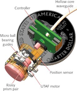
When miniaturizing optical instruments for portable use, making the light source, optics, detector, and electronics as small as possible isn't enough—the design engineer must also know what options are out there for compact mechanics. For example, micro beam-steering systems need to be very small, operate on battery power, and resist shock and vibration. For many uses, they should also rapidly move optics with milliradian precision in any orientation and work over wide temperature ranges. Engineers at New Scale Technologies (Victor, NY) have developed different approaches to beam steering that meet these requirements, including two-mirror, one-mirror, and Risley-prism-based devices (see Fig. 4). (See "Precision micro beam-steering systems simplify move to handheld instruments," LFW, July 2015; http://bit.ly/1MAiGLu.)14. Lasers can repair optics.
The largest laser system in the world—the National Ignition Facility (NIF), which is overseen by Lawrence Livermore National Laboratory (LLNL; Livermore, CA)—places high demands on its fused-silica optics. In fact, the near-IR laser's high irradiance levels can damage some of the optics, creating small pits in the surface. Scientists at NIF are using lasers to repair this damage. By varying the wavelength, power, beam size, or pulse duration of the repair laser, the nature of the optics-healing interaction can be controlled and fine-tuned. Techniques being looked at include IR pulsed laser micromachining, laser chemical vapor deposition (L-CVD), and a 3D printing additive process called selective laser melting (SLM). Exploring the effectiveness of these approaches requires extensive simulation in the form of multiphysics modeling of both the properties of the optical material and the laser's attributes. (See "Processing optics using IR lasers," LFW, August 2015; http://bit.ly/1E7n5bt.)
15. CMOS and CCD become as one.
Discussions abound on whether a CCD or a CMOS imager is the best choice for a particular application. But these technologies can and have been combined in the form of a monolithic system-on-chip CCD platform developed at ESPROS Photonics (Sargans, Switzerland) that is completely integrated within a CMOS environment. The combination provides a full scope of analog mixed-signal and digital design options on a less-complex CMOS platform. Backside illumination and a thick detector volume allow for order-of-magnitude sensitivity improvements as illustrated by a near-IR time-of-flight camera-on-chip useful for distance monitoring in industrial-scale applications. (See "CMOS and CCD combine in NIR time-of-flight on-chip imager," LFW, August 2015; http://bit.ly/1PBLMxV.)
16. Laser Doppler detects melanoma.
Laser-Doppler velocity detection can be used for studying the mechanics of the ear, measuring the distance between the blade tip of a turbine rotor and its housing, and monitoring the heart. Now, it could be put to use in the fight against melanoma, one of the deadliest forms of cancer. Researchers at Pisa University (Italy) and Lancaster University (England) are using a laser Doppler system to detect the subtle differences in blood flow beneath the skin between malignant melanoma and noncancerous moles (which can look very much alike, especially in the early stages of melanoma; see Fig. 5). Because melanoma tumors show quick blood-vessel growth, the resulting differences in blood flow between healthy and malignant moles are detectable. In fact, the test identified melanoma in all cases where it was present, and produced less than 10% false positives. (See "Laser Doppler records blood flow to enable early melanoma detection," LFW, September 2015; http://bit.ly/1LQiHOg.)
17. Laser eye test detects Alzheimer's.
Early intervention and treatment of Alzheimer's disease are the only way to slow the progression of the condition. Rather than subjective judgements, objective ways to diagnose the disease are needed. Based on recent discoveries about the close connection between the eye and the brain, a noninvasive, low-cost, biophotonics-based test has been developed by researchers at Cognoptix (Acton, MA) to diagnose Alzheimer's at the point of care. Because amyloid beta, which is crucial to the onset and progression of the disease, has been found to appear in the lens of the eye, an amyloid-binding ligand is administered to the inner eyelid the day before the laser-based test. When the eye is laser-scanned, any ligand/amyloid complex present fluoresces in proportion to its amount. The scan takes only a second to perform and, in a clinical trial, showed 85% sensitivity and 95% specificity in predicting probable Alzheimer's disease. (See "Laser-based eye test for early detection of Alzheimer's," LFW, September 2015; http://bit.ly/1NeAhcB.)
18. Optical filter, simplified.
Transmissive bandpass filters for the visible region can be made in numerous ways: a piece of colored glass or plastic, a multilayer film on a substrate, or even an array of plasmonic nanoholes. If the bandpass must be narrow, colored glass is out and multilayer interference filters are the norm. Now, a new configuration can be added: a single layer of glass sandwiched between two silver films, called a metal-insulator-metal (MIM) Fabry-Perot cavity. Developed by a group at Northwestern University (Evanston, IL), the filter depends on the optical loss in the top layer of silver for its narrowband properties. With a 60% peak transmittance for its 40 nm bandwidth, this filter is not going to compete with the best multilayer filters. However, the MIM filter is much cheaper to make. (See "Simple three-layer silver-glass-silver optical structure serves as narrowband spectral filter," LFW online, February 16th; http://bit.ly/1DlBPBL.)
19. Graphene becomes incandescent light source.
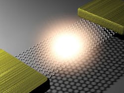
While III-V semiconductor lasers can serve as hybrid light sources in silicon photonic circuits, another approach has emerged—one that goes back to the days of Thomas Edison, who made his first incandescent light bulbs with carbon filaments. Scientists from Columbia University (New York, NY) and their colleagues from other institutions have updated Edison's invention by using graphene instead of carbonized bamboo and placing it on a silicon chip rather than an evacuated bulb (see Fig. 6). The graphene strip, which spans two conducting contacts, reaches temperatures of above 2500°C when conducting an electrical current. Interestingly, the light emitted by the graphene deviates from a blackbody spectrum because of interference between the light emitted directly from the graphene and light reflecting off the silicon substrate and passing back through the graphene. In addition to being light sources for integrated photonics, the glowing graphene strips could possibly be integrated into flexible substrates for other uses. (See "Graphene becomes incandescent light source for use in integrated photonic circuits," LFW online, June 15th; http://bit.ly/1Pn37fi.)20. Submillimeter-sized optical gyroscopes.
While optical gyroscopes are an integral part of inertial-guidance systems for missiles, satellites, and space probes, as with many complex devices, they would find wider use if they were shrunk in size and weight. Researchers at the College of Staten Island, City University of New York and Yale University (New Haven, CT) have done just that, producing an optical-cavity-based gyroscope that relies on measuring the far-field emission of the cavity, allowing the cavity size to be reduced to about 10 μm. The microdisk cavity is shaped asymmetrically to emit a prescribed small amount of light into the far field, where it is detected by two cameralike detectors. The gyroscope can be integrated into a photonic circuit to form a chip-based navigation system. (See "Light-powered gyroscope has submillimeter dimensions," LFW online, April 1st; http://bit.ly/1Op7fgh.)
About the Author
John Wallace
Senior Technical Editor (1998-2022)
John Wallace was with Laser Focus World for nearly 25 years, retiring in late June 2022. He obtained a bachelor's degree in mechanical engineering and physics at Rutgers University and a master's in optical engineering at the University of Rochester. Before becoming an editor, John worked as an engineer at RCA, Exxon, Eastman Kodak, and GCA Corporation.
