Mid-infrared Lasers: CMOS silicon-on-sapphire process produces broad mid-IR supercontinuum
Beyond its well-known photonic capabilities in the telecommunications wavelength band around 1.5 μm and its functionality in silicon-on-insulator (SOI) form up to 2.5 μm, silicon has now entered a new frontier: silicon-on-sapphire (SOS) nanowires have been used to demonstrate octave-spanning mid-infrared (mid-IR) supercontinuum generation from 1.9 to just beyond 6 μm.1
This broadband supercontinuum source is realized using a complementary metal-oxide semiconductor (CMOS) process and is the collaborative effort of researchers from the Center for Ultrahigh Bandwidth Devices for Optical Systems (CUDOS) at the University of Sydney, Macquarie University, and Silanna Semiconductor (all in Sydney, NSW, Australia), the CUDOS Laser Physics Center at Australian National University (Canberra, ACT, Australia), the Institut des Nanotechnologies de Lyon, CNRS (Lyon, France), and RMIT University (Melbourne, Victoria, Australia). The team of researchers says that this mid-IR supercontinuum source represents "both the widest spectrum and longest wavelength generated to date in any silicon platform."
Compact, inexpensive mid-IR sources are becoming more and more important, especially for applications in molecular sensing at part-per-billion and even part-per-trillion levels. Although supercontinuum generation using chalcogenide glass fibers has been demonstrated out to 13 μm, the CMOS-compatible SOS platform offers scalability and promises new nonlinear integrated (and cost-effective) silicon devices such as this mid-IR supercontinuum source that operates well beyond the legacy silicon window.
Supercontinuum SOS
The first SOS waveguides fabricated in 2010 had 4.3 dB/cm losses at 4.5 μm.2 To avoid higher multiphoton absorption that normally occurs in silicon beyond 2.5 μm, the researchers engineered SOS nanowires that minimized dispersion and optical loss at the pump wavelength via a 2.4 × 0.48 μm nanowire. By treating the nanowire with chemical oxidation and oxide stripping to reduce surface roughness, and by using a relatively wide nanowire to improve mode confinement, propagation losses are minimized to a level of 1.0 ± 0.3 dB/cm at 4 μm.
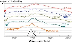
For supercontinuum generation, the 3.7 μm, 320 fs pulse-width, 20 MHz repetition rate output from a tunable optical parametric amplifier (OPA) was input to the TE mode of the nanowire, collimated and sent to a monochromator, and detected with two detectors: lead selenide (PbSe) from 1.5 to 4.8 μm and mercury cadmium telluride (MCT) from 4 to 6.5 μm. For coupled input peak powers from 200 W to 2.5 kW, the widest continuous output spectrum spans 1.53 octaves from 1.9 to 5.5 μm at the -30 dB signal level for a 1.82 kW input. Even well above the noise floor at -45 dB, light is generated beyond 6 μm (see figure).
To achieve a flatter dispersion profile over a wider bandwidth, SOS-based pillar waveguides could be constructed. Furthermore, improvements to epitaxial growth of the SOS nanowires are expected to minimize near-IR losses by reducing lattice mismatch at the silicon/sapphire interface. The researchers say that these improvements will make it possible to demonstrate supercontinuum generation over the full transparency spectrum of silicon using a single nanowire.
"The silicon-on-sapphire platform paves the way for integration of electronics and photonics on a single device," says Neetesh Singh of CUDOS, University of Sydney. "This would lead to electrically tunable, on-chip, linear, and nonlinear ultrawide optical operation from near-IR to mid-IR range."
REFERENCES
1. N. Singh et al., Optica, 2, 9, 797–802 (September 4, 2015).
2. T. Baehr-Jones et al., Opt. Express, 18, 12, 12127–12135 (2010).
About the Author

Gail Overton
Senior Editor (2004-2020)
Gail has more than 30 years of engineering, marketing, product management, and editorial experience in the photonics and optical communications industry. Before joining the staff at Laser Focus World in 2004, she held many product management and product marketing roles in the fiber-optics industry, most notably at Hughes (El Segundo, CA), GTE Labs (Waltham, MA), Corning (Corning, NY), Photon Kinetics (Beaverton, OR), and Newport Corporation (Irvine, CA). During her marketing career, Gail published articles in WDM Solutions and Sensors magazine and traveled internationally to conduct product and sales training. Gail received her BS degree in physics, with an emphasis in optics, from San Diego State University in San Diego, CA in May 1986.