Single-Photon Counting: Photonic integration meets single-photon detection
ALEXANDER KORNEEV, GREGORY GOLT'SMAN, and WOLFRAM PERNICE
The overwhelming success of integrated circuits (ICs) is largely a result of controllable and highly optimized fabrication that provides scalable production conditions. Complex systems can be realized by arranging individually designed and optimized components in circuit form. Interconnection between the individual building blocks is achieved with electrical wires for electrical signal exchange and ICs can be replicated with high yield and low cost because the micro- and nanofabrication routines used are inherently designed for mass production.
In direct analogy to electrical circuits, a similar route has been followed for designing optical systems out of micro-fabricated photonic components. Nanophotonic waveguides take on the role of electrical wires to connect functional elements into nanophotonic integrated circuits (NPICs) that find a multitude of applications for optical signal processing and optical sensing.
Besides applications in classical optics, NPICs also enable more exotic applications: using only waveguide-based photonic devices, the on-chip equivalent of free-space optical components can be readily implemented, offering a new route towards scalable linear optical quantum computing.1 In this case, NPICs are used to route and process single photons in contrast to the relatively high optical intensities used for telecommunication applications.
For full-scale on-chip quantum circuits, both passive waveguides and filter elements must be integrated with active single-photon sources and integrated single-photon detectors. A monolithic implementation of these quantum-photonic-circuit building blocks can overcome the stability and scalability limitations that plague bulk-optic realizations.
NPIC-based single-photon detector metrics
To date, we have evaluated several performance metrics for optimal NPIC-worthy single-photon detectors. The three most desired features-low dark-count rate (Rdc), high detection efficiency (DE), and accurate timing resolution-can be conveniently joined by analyzing the noise equivalent power (NEP).2
Detectors with low NEP are increasingly sought after for applications in both quantum and classical technology because they can be used during long measurements with high signal-to-noise ratio (SNR). For example, quantum key distribution has for a long time been limited in rate and range by imperfect detector characteristics. Fortunately, superconducting nanowire single-photon detectors (SNSPDs) can provide new alternatives.3
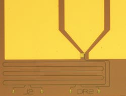
Today's SNSPDs are made from ultrathin superconducting films typically with a thickness below 5 nm that are patterned lithographically into narrow nanowires on the order of 100 nm width. Traditionally, the nanowires are arranged in a meander pattern and then illuminated with single photons by coupling to optical fiber. The detection mechanism relies on single-photon-induced loss of superconductivity in a nanowire that is current-biased close to its critical current. The detection process combines short recovery time and high quantum efficiency both for visible and infrared wavelength photons, thus providing broadband detection capability covering, in particular, the telecommunication bands.
State-of-the-art SNSPDs are predominantly stand-alone units absorbing photons under normal incidence. Because the nanowire meanders are prepared from ultrathin films the optical absorption in a single pass is limited, which in turn limits the overall detection efficiency. To increase photon absorption several approaches exploiting optical cavity implementation have been realized recent in years. The most successful one provides almost unity absorption within SNSPD meanders at the cost of reduced optical bandwidth.4 However; even though cavity integrated SNSPDs will surely evolve as stand-alone detectors, they are not very suitable for NPICs.
Better superconductors
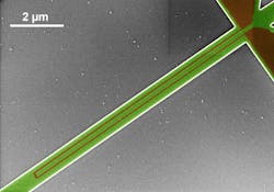
The reduced bandwidth and other shortcomings of cavity based SNSPDs can be overcome by fabricating traveling-wave superconducting nanowire detectors directly on top of nanophotonic waveguides (see Fig. 1).5,6 In such devices photons propagate underneath the superconducting nanowire, drastically increasing the interaction length to essentially achieve unity absorption efficiency. This in turn translates into high on-chip detection efficiency.
Depending on the material system from which the waveguides are prepared, different wavelength regimes can be targeted. In silicon photonic NPICs wavelengths above 1100 nm can be guided and detected. When broader wavelength access is required, related materials such as silicon nitride (Si3N4) can be used to enhance the detection window for visible and near-infrared wavelengths.7
In terms of superconducting materials suitable for SNSPD manufacture, niobium nitride (NbN) has been an attractive candidate, offering high critical temperatures above the boiling point of liquid helium and not requiring dilution refrigeration.8 Other superconducting materials that have recently been investigated for single-photon detection include tungsten silicide (WSi), molybdenum silicide (MoSi), tantalum nitride (TaN), niobium (Nb), and niobium titanium nitride (NbTiN).
Amorphous silicides, which are not very sensitive to the quality of the substrate surface, are suitable for integration with optical cavities, dielectric mirrors, and antireflective coatings for improving the detection efficiency. Although a record DE of 93% was demonstrated with cavity-integrated WSi SNSPDs, these materials have several drawbacks; namely, their low critical temperature leads to a low response pulse magnitude that results in increased timing jitter. Also, they feature longer response times compared to NbN. Both NbTiN and NbN provide similar superconducting properties and similar performance in terms of detection efficiency and dark count rates.
Detector integration
Using various superconducting materials, we have prepared functional detector devices using high-resolution electron beam lithography combined with reactive ion etching to structure each of the involved material layers, including the superconducting thin film as well as the waveguide material. By engineering the detector and waveguide dimensions at the nanoscale, highly efficient single-photon detection with high timing accuracy and low dark count rate is achieved. The resulting waveguide-integrated detectors feature very low NEP on a fully scalable platform.
The design concept for our SNSPDs can be applied in principle to any material system that supports guidance of optical modes, including silica, III-V semiconductors such as gallium arsenide (GaAs), or even lithium niobate.9 Since the optical circuits are fabricated with established fabrication recipes, they feature high reproducibility which means that the performance of each circuit component can be calibrated accurately. In our silicon photonics detectors we achieve a maximum on-chip detection efficiency of 91% for photons at 1550 nm input wavelength.
Using silicon nitride waveguides we also explored detection efficiency at 780 nm. For equivalent detectors made from NbTiN we find a maximum efficiency of 82%. By decreasing the nanowire width to 60 nm we further observe clear plateau behavior at higher bias current, which implies ultrahigh internal quantum efficiency.
Besides high detection efficiency, our detectors feature background-limited dark count rates. That means in practical detectors the minimum dark count level is restricted by the residual thermal-radiation photons that are generated in the room-temperature part of the input optical fiber. Meanwhile, if the SNSPD is efficiently shielded from the background, minimum dark counts rate may be as low as 2 × 10⁻⁴ Hz,10 resulting in NEP of 5 × 10-21 W⁄√Hz 1550 nm wavelength.
When proper filtering is applied, the dark count rate in practical systems can be reduced below 0.1Hz. For the silicon waveguide integrated NbN detectors we obtain minimal dark count rates of 50 Hz when approaching the critical current. Using NbTiN, this dark count rate can be further reduced to measured rates in the millihertz range.
Since the waveguide-integrated detectors are fabricated with a small device footprint, the overall meander length is significantly shorter than in traditional fiber-coupled SNSPDs. This results in an equivalent reduction of the kinetic inductance of the detector and thus reduced reset time. For the silicon-based detector devices we find a minimum relaxation time of 500 ps, which allows for single-photon detection rates above 1 GHz. Furthermore, the devices provide very low timing jitter below 20 ps which is attractive for on-chip time-resolved measurements.On-chip multiphoton detection
An emerging application for waveguide-integrated detectors is for multiphoton detection. By engineering both the nanowire width and the biasing conditions, desired detection capabilities can be chosen by the user.
When operating superconducting nanowires with wider meanders far from the critical current, the absorption of a single photon is not sufficient to induce a transition to the normal state. Therefore, such devices only lead to a detection event when simultaneous absorption of multiple photons occurs. In combination with on-chip optical cavities and multiplexing, specific photon distributions can be engineered that fit the detection regime of the nanowire, thus offering a promising route towards on-chip multiphoton detection.
Waveguide-integrated superconducting single-photon detectors are promising devices because they combine many desirable detector properties all in a compact optical component. Particularly attractive is the high timing resolution, as well as the very low dark count rate and hence low NEP. Because waveguide-integrated single-photon detectors can be fabricated with high yield and uniform performance across a large area, they are prime candidates for multi-detector architectures. Along with recent advances in on-chip single-photon sources, integrated single-photon detectors bring together all the required elements needed for future applications in integrated optical quantum computing.
REFERENCES
1. J. L. O'Brien, A. Furusawa, and J. Vuckovic, Nature Photon., 3, 12, 687–695 (2009).
2. R. H. Hadfield, Nature Photon., 3, 12, 696–705 (2009).
3. G. Goltsman et al., Appl. Phys. Lett., 79, 6, 705–707 (2001).
4. F. Marsili et al., Nature Photon., 7, 3, 210–214 (2013).
5. J. P. Sprengers et al., Appl. Phys. Lett., 99, 181110–181112 (2011).
6. W. H. P. Pernice et al., NatureCommun., 3, 1325 (2012); http://dx.doi.org/10.1038/ncomms2307.
7. C. Schuck, W. H. P. Pernice, and Hong X. Tang, NatureSci. Rep., 3, 1893 (2013); http://dx.doi.org/10.1038/srep01893.
8. A. Verevkin et al., Appl. Phys. Lett., 80, 25, 4687–4689 (2002).
9. M. G. Tanner et al., Nanotechnology, 23, 50, 505201 (2012).
10. A. Korneev et al., Appl. Phys. Lett., 84, 26, 5338–5340 (2004).
Alexander Korneev is a senior researcher and Gregory Golt'sman is a professor of physics and scientific adviser, respectively, in the Radiophysics Laboratory at Moscow State Pedagogical University, 29 Malaya Pirogovskaya St., Moscow, 119435, Russia and at SCONTEL, 5/22-1 Rossolimo St., Moscow, 119021, Russia; http://eng.mpgu.edu and http://www.scontel.ru. Wolfram Pernice is a professor of physics in the Department of Physics at the University of Münster, Wilhelm Klemm Str. 10, 48149 Münster, Germany; e-mail: [email protected]; http://www.uni-ms.de.


