Lasers for 3D Printing: Additive manufacturing with NIR lasers forms micro-sized parts
FABIAN NIESLER, MARTIN HERMATSCHWEILER, and ANKE WERNER
Additive manufacturing (AM) or three-dimensional (3D) printing is hitting the headlines with ever-spectacular developments. While AM has been used for years as the de facto standard for rapid prototyping in architectural, aerospace, and engineering applications, the technology has disruptive potential for mass-produced, final-parts production in a variety of industries.
Driven by the general trend of miniaturization, there is a growing demand for high-resolution 3D printers. On the micrometer scale, AM or 3D printing overcomes size and shape complexity constraints in conventional manufacturing methods and enables the fabrication of micro-scaled parts.
Why laser lithography?
Known for its high precision with typical layer thicknesses in the range of 50 to 150 μm, stereolithography is the process by which a vat of liquid ultraviolet (UV)-light-curable photopolymer is polymerized by a UV laser in a layer-by-layer fashion. But when stereolithography—also called vat photopolymerization—reaches its limitation with respect to resolution, 3D multiphoton lithography can be used to fabricate objects with heights up to several millimeters and layer thicknesses well below 1 μm.
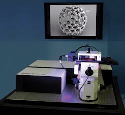
Seven years ago, scientific pioneers in the field of laser lithography developed the first commercially available 3D laser lithography system and founded the company Nanoscribe as a spin-off of the Karlsruhe Institute of Technology (KIT; Karlsruhe, Germany). The company has since developed 3D multiphoton lithography systems such as the Photonic Professional GT, a microprinter for fabrication of 3D microstructures and nanostructures used in photonics, microfluidics, micro-optics, rapid prototyping, and life science/bioengineering applications.
Parts fabrication
The direct laser-writing technique underlying the 3D printing method is based on two-photon polymerization of photopolymers. In this process, near-infrared (NIR) ultrashort laser pulses spatially cure photosensitive materials when a certain intensity threshold is reached. The light-induced polymerization is triggered only in the focal point volume, the so-called voxel.
The resolution of the process as well as the voxel size are mainly determined by the laser spot size in the material, the power of the laser source, and the properties of the photosensitive material itself. By using focusing optics with a high numerical aperture, very small voxels with sub-micrometer dimensions can be achieved.
To move the voxel relative to the sample, two technical implementations can be distinguished. In the fixed-beam moving-sample approach, the substrate is moved in all three dimensions by a high-precision positioning unit relative to the focusing optics. This movement is driven by piezoelectric actuators that allow for a very precise focus trajectory. Almost arbitrarily complex-shaped polymer structures with the finest lateral feature sizes in the sub-micrometer range and a vertical resolution of typically 1 μm are achieved.
Dramatic speed increases in the printing process can be achieved if the laser beam is laterally scanned by galvanometric mirrors. This moving-beam fixed-sample approach allows for much faster fabrication using a layer-by-layer build-up process. To ensure the highest precision even at high writing speeds, an accurate coordination of beam deflection, sample movement, and laser intensity modulation must be secured at all times during the writing process.
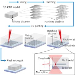
For parts fabrication, the desired structures can be designed in 3D-printer-compatible CAD software and transferred as STL files into the laser lithography system. An automatic process of mesh fixing (the mesh being a digital file of triangular shapes with vertices, edges, and faces that form the 3D object) eliminates typical mesh errors such as missing triangles that form voids in the object surface. Slicing and hatching routines then generate the trajectories for the laser focus (see Fig. 1).
After the printing process, the crosslinking of polymer chains renders the exposed volume insoluble relative to its unexposed environment. The unexposed material is removed in a developer bath and the exposed regions remain as self-supporting 3D microstructures and nanostructures.
Materials
A wide range of materials with different optical, mechanical, electronic, and chemical/biological properties has been validated successfully for direct laser writing. The list of compatible resists or resins includes standard photopolymers such as SU-8 (well known in the semiconductor industry) or Ormocere (used in the field of bioengineering). Nanoscribe also develops its own resists to provide maximum 3D-printer performance with respect to resolution, writing speed, structural accuracy, and ease of use along the process chain.
Polymer structures can be printed on a variety of substrates with different chemical and physical properties. The choice of the right substrate material depends on the type of application. For use in optical applications, transparent substrate materials such as glass or pre-structured substrates like opaque semiconductor wafers or transparent microfluidic chips can be used. Laser lithography is an elegant way to combine the substrate with optical or mechanical components to enhance functionality.
Despite numerous two-photon-polymerization-compatible photopolymers, there remain many classes of non-polymerizable materials that cannot be used to fabricate 3D structures in a one-step-procedure. However, there are different post-processing techniques that replicate 3D polymer parts using other materials including metals, silicon, silica, or polydimethylsiloxane (PDMS).
Stronger and lighter
In 2012, the European Factories of the Future Research Association (EFFRA; http://www.effra.eu) highlighted AM as a means to realize larger-scale targets such as creating sustainable high-value European-based employment, addressing societal issues, and supporting environmental sustainability and innovation for manufacturing.1
In addition to AM and 3D printing, nanotechnology is also a driver of innovation. The combination of both technologies has the potential to meet many challenges. Therefore, 3D printers for micrometer-scale objects are becoming a valuable tool for R&D within various scientific and industrial topics including materials research, optical interconnections, and micro-optics.
Recently, material researchers have developed functional materials with improved performance and totally new properties using 3D multiphoton lithography. Complex 3D microtrusses or "mechanical metamaterials" have been printed, allowing a massive reduction of weight. By tailoring the shape, size, orientation, and arrangement of unit cells, an ultra-lightweight porous material with unconventional effects on the propagation of sound waves can be created.2
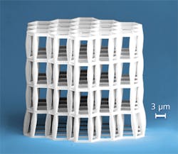
By learning from nature, researchers are challenging common wisdom that says strong materials are heavy and light materials are weak. Nanoscale 3D microprinting can create a bone-like material that is as strong as steel, yet is lighter than water (see Fig. 2). "Strength and density, two material properties of central relevance for engineering, are generally considered as strongly coupled," says Jens Bauer from KIT. "However, nature shows us how we may overcome long-standing barriers in the search for light yet strong materials." Cancellous (spongy) bone and other natural cellular solids have an optimized architecture, designed adaptively to the loading situation while at the same time keeping the overall weight as low as possible.At the lowest hierarchical level, bone consists of nanometer-sized building blocks for enhanced material strength because of mechanical-size effects. Designing cellular materials with a specific microarchitecture allows one to exploit both structural advantages and size-dependent strengthening mechanisms. Besides bone, researchers have also applied 3D direct laser writing to micro-architect lightweight materials from ceramic-polymer composites. Mechanical characterization of the fabricated structures verifies outstanding strength-to-weight ratios comparable to high-performance steels and technical ceramics.3
Direct laser writing has also been used to replace conventional electronics with higher-performance optical circuits. Record-breaking data transmission rates of more than 5 Tbit/s are possible using nanophotonic interconnected technology based on photonic wire bonds (PWBs) written using laser-induced two-photon polymerization, a promising solution to overcome communication bottlenecks in datacenters and high-performance computers.4
Laser direct writing is also finding use in life-science tissue engineering. Using 3D laser lithography, freely designed cell scaffolds can be created (see Fig. 3). The influence of the physical environment (stiffness and architecture) on stem-cell differentiation or cell migration can be investigated. Research studies have shown that the behavior of living cells embedded in these artificial extracellular matrices is similar to behavior in the natural environment, which has important ramifications for the investigation of tissue regeneration or toward understanding the influence of active pharmaceutical ingredients on wound healing, for example.In summary, 3D printing will establish itself in many fields of nano- and microtechnology. Research institutes and universities around the world are already using 3D printers for the micrometer scale and are appreciating their performance and quality. Now, the time has come to transfer the benefits to R&D departments within the industry.
REFERENCES
1. European Union "2013 Additive Manufacturing: Strategic Research Agenda"; see http://www.rm-platform.com/linkdoc/AM%20SRA%20Consultation%20Document.pdf.
2. M. Kadic et al., Appl. Phys. Lett. 100, 191901 (2012).
3. J. Bauer et al., Proc. of the National Academy of Sciences (PNAS) 111, 7, 2453–2458 (2014).
4. N. Lindenmann et al., Opt. Express 20, 17667 (2012).
Fabian Niesler is head of Processes & Applications, Martin Hermatschweiler is CEO, and Anke Werner is marketing manager at Nanoscribe, Hermann-von-Helmholtz-Platz 1, Eggenstein-Leopoldshafen, 76344 Germany; email: [email protected]; www.nanoscribe.de.


