Thumb-drive-sized spectrometer achieves subnanometer resolution
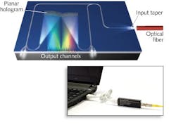
Nano Optic Devices (Santa Clara, CA, and Troitsk, Russia) has developed a chip-based spectrometer that is not only very compact, with packaged dimensions comparable to a typical USB thumb flash drive, but also achieves the subnanometer resolution typically found in larger laboratory-grade spectrometers the size of a laptop power supply. The new spectrometers use digital planar holography (DPH) technology fabricated using CMOS processing to micro-engineer phase and polarization characteristics that manage and guide light beams inside a chip more efficiently than bulky traditional optics. The technology allows for automated nanoimprint-lithography production techniques with low manufacturing costs and high-reproducibility, solid-state optics that never need recalibration, and are insensitive to temperature, humidity, and vibration.
The DPH spectrometer core consists of millions of grooves ranging in width from several dozens to several hundred nanometers fabricated at the surface of a planar waveguide. These diffractive devices perform spectral decomposition of the input light (delivered through an optical fiber) by focusing the different spectral components at locations along the chip output where a linear CCD detector array is installed. Custom devices can be fabricated to operate in wavelength ranges from 500 to 1100 nm and 1100 to 1500 nm. Current standard products include 600–690 nm and 630–690/760–850 nm wavelength ranges with 0.18 nm resolution, and a 760–920 nm device with 0.15 nm resolution. Contact Paul Murphy at [email protected].
About the Author

Gail Overton
Senior Editor (2004-2020)
Gail has more than 30 years of engineering, marketing, product management, and editorial experience in the photonics and optical communications industry. Before joining the staff at Laser Focus World in 2004, she held many product management and product marketing roles in the fiber-optics industry, most notably at Hughes (El Segundo, CA), GTE Labs (Waltham, MA), Corning (Corning, NY), Photon Kinetics (Beaverton, OR), and Newport Corporation (Irvine, CA). During her marketing career, Gail published articles in WDM Solutions and Sensors magazine and traveled internationally to conduct product and sales training. Gail received her BS degree in physics, with an emphasis in optics, from San Diego State University in San Diego, CA in May 1986.