MID-INFRARED OPTICS: CVD diamond IR optics enable EUV lithography
ANDREW BENNETT, EUGENE ANOIKIN, and BENNO VROLIJK
For more than 40 years, the well-known Moore's Law has been behind the optical lithography industry's push toward more powerful and energy-efficient computer chips. One of the key approaches to producing ever-smaller transistors is to take advantage of ever-shorter wavelengths of light in optical lithography. The latest transition is from deep-ultraviolet (DUV) light at 193 or 248 nm to extreme-ultraviolet (EUV) light at only 13.5 nm.1 There are limited ways of producing this light efficiently, with the frontrunner being emission from tin-based laser-produced plasma (LPP) pumped by carbon dioxide (CO2) lasers.
While many fundamental engineering issues have been resolved, these plasmas emit at the required wavelengths with low efficiency; in addition, once the light is emitted it is hard to manipulate without high system losses. This creates a challenge in introducing sufficient power into the plasma to enable rapid wafer processing rates—the average input IR pump power into the system must typically be higher than 20 kW, with pulse energies of up to 1 J at pulse durations of down to 10 ns—levels that have rarely been required in more-traditional laser applications.
Some CO2 lasers with appropriate average-power outputs are available; however, they need to be switched to produce the desired pulse shapes, leading to further inefficiencies. In practice, multiplexing of two or more high-power outputs is required for LPP extreme UV (EUV) systems. One challenge with the sort of laser powers being used is that traditional material solutions for the optics are either entirely insufficient or have short lifetimes. In addition, the environment around the plasma has significant debris, which further limits the performance of traditional materials.
Diamond properties
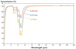
Diamond has long been known to have exceptional properties, largely resulting from the symmetry of the cubic lattice made of light carbon atoms connected by extremely strong bonds. It has historically been exploited mainly for its great hardness in mechanical applications; however, it has also been used where its sensing, thermal, or semiconducting properties are useful. As long ago as 1978, diamond was being used for optics. For example, diamond was used in the Pioneer Venus Orbiter spacecraft as a window for its infrared (IR) spectrometer due to its wide window of transparency (see Fig. 1) and excellent mechanical properties.2 However, natural diamond is not typically available in the sizes necessary for optics, nor in the consistent quality required for engineering solutions.
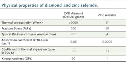
To investigate the value of diamond for LPP EUV applications, it is useful to list the key specifications for optics in high-power beamlines: 1) low absorption coefficient; 2) high fracture strength; 3) high thermal conductivity; and 4) low coefficient of thermal expansion (CTE). The table compares some physical properties of diamond with those of a commonly used IR optical material, zinc selenide (ZnS).Low absorption is critical to minimize heating of optical components, as well as the optical loss in the overall system. Diamond has a wide bandgap of 5.45 eV, meaning the short-wavelength cut-off for diamond is around 230 nm, while the material is largely transparent well into the microwave region due to the symmetry of the bonding. As a result, diamond has good transmission across a wide range of wavelengths, including many of the key wavelengths that may be used for powering EUV systems.3 Of course, it should be noted that polycrystalline diamond is being used. In many optical materials, the polycrystalline nature of the optical element would limit its use; however, diamond's cubic structure minimizes the impact of multiple crystalline orientations in the film on performance.
The second key feature of diamond is its high fracture strength. When optics serve as dividers between volumes of differing pressure, this can become critical. A typical diamond window designed to safely hold a pressure can be more than four times thinner than a similar window made from ZnS. This higher fracture strength will clearly reduce the total absorbance in the system, mitigating the slightly higher absorption coefficient of the diamond window over competitor materials.4
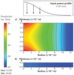
The next key parameter of the system is the thermal conductivity. All the absorbed power in the window must be rapidly moved out to the cooling system to minimize the window's peak temperatures, which can lead to power loss through thermal lensing, or to breakage of optics. This heat comes not only from the bulk window material, but also from coatings, which can have higher absorption coefficients than the window itself. As a result, the practical importance of good thermal conductivity can be higher than that of low absorption. Here, diamond excels; the stiffness of the bonds and the lightness of carbon atoms mean that the lattice has extremely high vibrational frequencies and a high Debye temperature of 2220 K. As applications tend to operate at well below this temperature, there is little phonon scattering. Diamond has the highest thermal conductivity of any solid at room temperature—at higher than 2000 W/m K, it is two orders of magnitude greater than key competitor materials (see Fig. 2).Finally, the low CTE of diamond is extremely useful to optical engineers. Even when some heating does occur to diamond windows, the low CTE ensures that the windows do not significantly alter their shape, minimizing thermal lensing and leading to large improvements in beam quality over competitor materials.
Synthetic diamond
The natural diamond used in the Pioneer Venus Orbiter is obviously not a solution for most optics engineers. For more than 50 years, synthetic diamond has been manufactured using high-pressure and high-temperature (HPHT) techniques, simulating conditions found in nature in which natural graphite is converted into diamond. For most commercial HPHT materials, the defect content is moderately high—for example, standard parts typically have >50 parts per million (ppm) of nitrogen (the most common impurity in diamond) in the lattice, which increases absorption at a range of wavelengths. As a result, commercial HPHT materials are more commonly used in applications that exploit the material's extreme hardness and wear resistance.
An alternate method of making polycrystalline and single-crystal diamond—chemical vapor deposition (CVD)—has become commercially viable over the last 15 years. In this process, gas-phase carbon is added to hydrogen at a level of a few percent into the growth tool and heated by microwaves to temperatures greater than 2000 K to dissociate the feedstock gases. This creates reactive carbon that becomes part of the growing diamond layer, but also creates a flux of atomic hydrogen radicals at the growth surface, stabilizing the growing diamond and etching away any impurities that are formed. With carefully controlled feedstock gases and good system design, in addition to tightly controlled process conditions, this has made possible the highest purity diamond, with, for example, background nitrogen-defect levels in single-crystal diamond measured at less than 0.005 ppm.
Both single-crystal and polycrystalline optical windows are made using this technique. To date, state-of-the-art optical-grade polycrystalline windows can be made with diameters up to 130 mm and thicknesses greater than 2 mm. These polycrystalline windows typically have diamond grains around 100 μm in size at the growth surface, nitrogen content <0.1 ppm, and boron content <0.005 ppm. Most importantly for optical applications in the infrared, it has an absorption coefficient <0.07 cm-1 at 10.6 μm, while its fracture strength is > 800 MPa for the nucleation surface, and its room-temperature thermal conductivity is > 2000 W/mK.5
Diamond for materials processing
As mentioned above, optical-grade synthetic diamond is not a novel material. It has been sold as a window material for high power lasers for the last two decades, and is now a regular part of laser systems used, for example, to mark, weld, and cut sheet metal.6 There is every chance that we all own something that has been cut using a CO2 laser enabled by a synthetic-diamond window, quite often in our vehicles.
The windows are also a key part of microelectronics manufacturing, with hundreds of laser systems working in the industry to create structures in circuitry that cannot easily or commercially be produced by alternative means. They are even a key part of manufacturing solar panels and batteries for renewable energy applications. An important point is that these windows are engineered materials much like any other optic. They can be optimized and then repeatedly produced to specification.
Diamond innovations for EUV lithography
Optical-grade diamond is the only material that can enable the high input powers required to improve system throughput in EUV lithography. In fact, existing material grades are sufficient to form windows that, with properly designed coatings and cooling, can handle upwards of 50 kW average power without failure.
One of the additional challenges with EUV is the extremely high-quality optical components required as far as minimizing wavefront distortion and loss of beam quality. A typical CO2 laser output coupler made out of diamond has a flatness of around 1 to 2 λ (λ = 633 nm); however, components for EUV systems can require a flatness spec as tight as λ/2 across larger windows, and some reflective optics may require λ/30—a true challenge when processing such a hard, chemically inert material. Element Six has recently fabricated windows with flatness of better than λ/20 across a 47 mm aperture and has methods that can be extended to larger sizes.
While optical-grade synthetic diamond has been central to many developments in the high-power IR laser community (particularly at 10.6 μm) over the last 20 years, it is of note that the drive for the next generation of transistors to meet our thirst for data and data processing consistent with Moore's law has perhaps, at least for the Pioneer Venus Orbiter generation, provided unexpected new opportunities and challenges for synthetic diamond. The increasing number of application areas that demand the extreme performance of diamond has already led to a rapid increase in manufacturing capacity, with Element Six recently increasing production capacity by 50% across its sites in the UK and U.S.
REFERENCES
1. EUV sources for Lithography, edited by Vivek Bakshi, SPIE Press Monograph, PM149 (2006).
2. The properties of Natural and Synthetic Diamond, edited by J. E. Field, Academic Press, London, England (1992).
3. Optical Engineering of diamond, edited by Richard P. Mildren and James R. Rabeau, Wiley-VCH Verlag GmbH, Weinheim, Germany (2013).
4. C. S. J. Pickles, Diam. Relat. Mater., 11, 12, 1913–1922 (2002).
5. J. M. Dodson et al., "Single crystal and polycrystalline CVD diamond for demanding optical applications," Proc. SPIE, 8016 (2011).
6. D. H. Douglas-Hamilton et al., "Diamond as a high-power-laser window," J. Opt. Soc. Am., 64, 1, 36–38 (1974).
Andrew Bennett, Eugene Anoikin, and Benno Vrolijk are at Element Six, Santa Clara, CA; email: [email protected]; www.e6.com/optical.


