NOVEL MATERIALS: Few-layer dichalcogenides create photoluminescent triangles
Pennsylvania State University (Penn State; University Park, PA) researchers have succeeded in fabricating single- and few-layer metal dichalcogenide two-dimensional (2D) triangular microplatelets of tungsten disulfide (WS2) that photoluminesce at their edges (and at room temperature).1
It is known that monolayers of transition-metal dichalcogenides act as 2D semiconductor crystals—unlike insulating metallic graphene—with direct bandgaps in the visible spectrum. However, it has been difficult to date to isolate (or grow) single-atomic layers of these materials due to their natural tendency to form closed fullerene-like, stacked-layer geometries or nanotubes.
To create the single- and few-layer WS2 structures that indeed consist of a single sulfur-tungsten-sulfur (S-W-S) layer, the researchers synthesized the devices through sulfurization of ultrathin tungsten trioxide (WO3) films. Penn State professor of physics Mauricio Terrones says, “We were surprised we could grow these perfect and attractive morphologies of monolayered WS2.”
Zigzag source of photoluminescence
Each WS2 monolayer has a single layer of tungsten atoms hexagonally packed between two trigonal atomic layers of sulfur atoms. While bulk WS2 is an indirect-gap semiconductor with a bandgap of 1.3 eV, it transitions (as layers are removed) to a direct-gap semiconductor in the monolayer form.
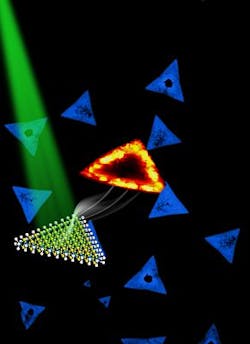
Fabrication of the triangular forms begins with depositing ultrathin films (5 to 20 Å thick) of WO3 on a silicon dioxide/silicon (SiO2/Si) substrate through thermal evaporation of a WO3 powder under vacuum. Upon exposure to a sulfur-rich atmosphere in a quartz-tube reactor at 800ºC, the thinnest films (5 to 10 Å) produce the early-stage films that eventually form into triangular islands of WS2 monolayers through W and S diffusion on the substrate. The triangles have zigzag-shaped edges of alternating W and S atoms, or pure W or pure S atoms. Elemental analyses show that only a small amount of oxygen remains and most of the WO3 is converted to WS2 triangular islands.
When the triangles are illuminated with 488 nm excitation, Raman spectroscopy confirms that monolayered triangles exhibit extraordinary room-temperature photoluminescence at the triangle edges. But as the number of layers increases, direct-gap dynamics give way to indirect gaps and luminescence is quenched.
While the photoluminescence mechanism is not entirely understood, it is linked to the concentration of excitons near the zigzag edges of the triangular islands. Penn State professor of physics Vincent Crespi says, “These tiny, atomically thin islands glow surprisingly strong from their edges. Normally, structural defects like edges would be expected to prevent light emission from devices: Light emission is a delicate thing, and defects tend to give excited electrons and holes ways to recombine without emitting light. Here, we see the opposite: The structural defect created by the edge of the device seems to be the favored place for emitting light.”
Terrones adds, “The edges are key in our observations; we are now studying—at the atomic scale—the edges of these triangles to determine precisely the types of atoms we have there. We are also measuring electronic transport on these edges and the triangles using different laser excitations.”
Potential uses
Because the sulfurization process can be customized to create a variety of monolayer structures, further research will continue on developing unique photoluminescent nano-optoelectronic 2D structures with possible uses in light emission and detection. Other applications in biology are possible; the chemistry occurring at the edges could also be very important for catalysis or photocatalysis.
REFERENCE
1. H.R. Gutiérrez et al., “Extraordinary Room-Temperature Photoluminescence in Triangular WS2 Monolayers,” to be published in ACS NanoLetters (2013).
About the Author

Gail Overton
Senior Editor (2004-2020)
Gail has more than 30 years of engineering, marketing, product management, and editorial experience in the photonics and optical communications industry. Before joining the staff at Laser Focus World in 2004, she held many product management and product marketing roles in the fiber-optics industry, most notably at Hughes (El Segundo, CA), GTE Labs (Waltham, MA), Corning (Corning, NY), Photon Kinetics (Beaverton, OR), and Newport Corporation (Irvine, CA). During her marketing career, Gail published articles in WDM Solutions and Sensors magazine and traveled internationally to conduct product and sales training. Gail received her BS degree in physics, with an emphasis in optics, from San Diego State University in San Diego, CA in May 1986.