Strain controls spontaneous emission in silicon nanowires
The direct bandgap due to quantum confinement, adjustable bandgap, sensitivity to surface ligands and mechanical excitation, and compatibility with mainstream silicon technology of silicon nanowires makes them excellent candidates for optoelectronic devices. Now, researchers at the University of Waterloo (Waterloo, ON, Canada), in collaboration with Texas A&M University–Kingsville and University of Washington–Seattle, have discovered that uniaxial strain can modulate the spontaneous emission of photons in silicon nanowires—a finding that improves the potential for these devices to function efficiently in a variety of optoelectronic applications, including a mechanism for lasing.
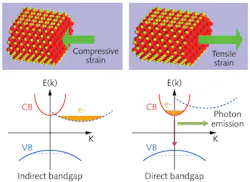
Using silicon nanowires ranging in diameter from 1.7 to 3.1 nm that have a direct bandgap at 0% strain, the researchers showed that compressive strain increased spontaneous emission time by one to two orders of magnitude. This occurs due to either the change of wave-function symmetry or direct-to-indirect bandgap conversion. To create a population inversion in silicon nanowires, current can be injected in a compressively strained nanowire with an indirect bandgap in which the light emission is a slow second-order process (mediated by phonons). During strain release or by applying tensile strain, the initial population can scatter into the direct sub-band via fast electron-phonon scattering processes. This initiates lasing if the nanowire is embedded in a suitable mode-enhancing cavity. Contact Daryoush Shiri at [email protected].
About the Author

Gail Overton
Senior Editor (2004-2020)
Gail has more than 30 years of engineering, marketing, product management, and editorial experience in the photonics and optical communications industry. Before joining the staff at Laser Focus World in 2004, she held many product management and product marketing roles in the fiber-optics industry, most notably at Hughes (El Segundo, CA), GTE Labs (Waltham, MA), Corning (Corning, NY), Photon Kinetics (Beaverton, OR), and Newport Corporation (Irvine, CA). During her marketing career, Gail published articles in WDM Solutions and Sensors magazine and traveled internationally to conduct product and sales training. Gail received her BS degree in physics, with an emphasis in optics, from San Diego State University in San Diego, CA in May 1986.