INTEGRATED PHOTONICS: High-contrast gratings forge ultralow-loss, slow-light waveguide
Pioneered by professor Connie Chang-Hasnain’s Group at the University of California–Berkeley, high-contrast gratings (HCGs)—alternating stripes of semiconductor materials and air (or silicon) with subwavelength periodicity—are an emerging integrated photonics platform being used to fabricate such diverse optoelectronic elements as reflective mirrors, lenses, high-Q resonators, vertical in-plane couplers, and even tunable vertical-cavity surface-emitting lasers (VCSELs). Now, the UC Berkeley team and scientists from the US Army Research Laboratory (ARL; Adelphi, MD) have worked further on the HCG platform to develop and experimentally demonstrate a hollow-core, slow-light waveguide with ultralow loss compared to devices made from conventional optical materials.
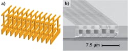
Four HCG walls
Unlike hollow-core waveguides made from homogeneous materials, the ultralow-loss waveguide is composed of four HCG “walls” that form a square, open structure with alternating silicon and air gaps for each HCG (see figure). Using modeling and simulation software developed at UC Berkeley, the dimensions and spacings of the waveguide metastructure are optimized for 100% reflection and zero core absorption. By engineering a phase transition that generates a zero slope in the dispersion curve (effectively, zero group velocity), the hollow-core waveguide is not only ultralow in loss, but is also engineered for high dispersion or “slow light” properties that are useful for creating long time delays or high-Q cavities for semiconductor-based, chip-scale integrated optoelectronic devices.
The 2D simulation model currently uses a pair of HCGs to optimize the physical parameters of the waveguide metastructure; however, a more complex 3D model is in development to finetune the waveguide parameters.
To fabricate the 3D waveguide from the 2D surface of a silicon-on-insulator (SOI) wafer, the researchers at ARL developed a new, self-aligned, “single” modified Bosch plasma-etching process that does not require complex multilayer deposition, regrowth, multilithography alignments, or wafer flip-bonding steps.1 The simplified fabrication process begins with a 2D etching mask (made by electron-beam lithography) placed on top of the SOI wafer. A series of dry and wet etching steps removes material exposed by the mask, creating the open structures that are the four HCG walls of the device.
Using an optimized metastructure waveguide with an open core height and width of approximately 1 μm and a line separation or period of approximately 0.7 μm, along with an approximate 1.5-μm-wide square frame for the HCG silicon structures or walls, the researchers at ARL fabricated waveguides with a variety of lengths that, incidentally, can even be peeled off the SOI structures and transferred to another substrate if desired.
Slow-light propagation
Preliminary waveguide test measurements were performed at ARL using the cutback method by focusing a tunable laser (1530–1560 nm) into the waveguides, demonstrating a propagation loss of less than -2 dB/cm for an approximately 12-mm-long waveguide. A group velocity of approximately 0.1 c (a tenth of the speed of light in vacuum) was observed by transiting a 1 ns short optical pulse through the waveguide.2
Weimin Zhou, leader of the RF-Photonics Team at ARL, says “These preliminary experiments proved for the first time that it is possible to obtain both slow light and low loss with this HCG waveguide. By improving our experimental techniques, we are hoping to obtain a group velocity less than 1% of the speed of light as predicted by UC Berkeley’s theoretical modeling. This will pave the way for fiber-like, low-loss long delay lines to be integrated into silicon ICs so that desirable high-Q devices are integrated into silicon chips for many RFPhotonic, data-processing buffer, and high-Q sensor applications.”3
REFERENCES
1. W. Zhou, U.S. Patent application #12/699,911,2010.
2. W. Zhou et al., Photonics West 2012, San Francisco, CA, paper 8270-08 (January 2012).
3. T. Sun et al., Photonics West 2012, San Francisco, CA, paper 8270-09 (January 2012).
About the Author

Gail Overton
Senior Editor (2004-2020)
Gail has more than 30 years of engineering, marketing, product management, and editorial experience in the photonics and optical communications industry. Before joining the staff at Laser Focus World in 2004, she held many product management and product marketing roles in the fiber-optics industry, most notably at Hughes (El Segundo, CA), GTE Labs (Waltham, MA), Corning (Corning, NY), Photon Kinetics (Beaverton, OR), and Newport Corporation (Irvine, CA). During her marketing career, Gail published articles in WDM Solutions and Sensors magazine and traveled internationally to conduct product and sales training. Gail received her BS degree in physics, with an emphasis in optics, from San Diego State University in San Diego, CA in May 1986.