PHOTOMULTIPLIER TUBES: Small-pore microchannel plates forge ultrafast photomultipliers
JON HOWORTH, JAMES MILNES, and GARETH JONES
Microchannel plates enable very fast electron amplification and are used in premium quality photomultiplier tubes (PMTs) for applications such as fluorescence lifetime measurements, with single-photon counting jitter down to 30 ps. The analog pulsewidth depends upon the pore size of the microchannel plate, and military night vision has driven down the pore size in an effort to improve resolution. Using these small-pore plates has resulted in faster photomultipliers that compete directly with streak cameras in applications as demanding as fusion diagnostics. Similar tubes used in particle accelerators have achieved multiphoton jitter of less than 10 ps.
Over the past ten years Photek has undertaken extensive developments in our microchannel plate (MCP)-based PMTs to improve and define their speed, dynamic range, and gating ability, making these devices critical assets in some of the most prestigious research facilities in the world.
Speed
The "speed" of a PMT is essentially the spread in time of the PMT output from a very short optical input—a theoretical delta function that in reality only has to be shorter in time than the PMT response. Given that a PMT generates many electrons from very few (or even just one) from the photocathode, the spread is minimized by trying to make all of the electrons arrive at the anode at the same time.
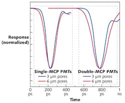
The MCP structure provides an ideal gain medium for this multiplication process, consisting of a thin glass disk (typically 0.3–0.5 mm thick) full of millions of holes known as pores. Electrons are accelerated down these pores, usually 6 or 10 μm in diameter, and are amplified on each bounce. The small structure of the MCP pores means that the possible variation of path length for each electron is very small, so the arrival time is similar for all-hence a very fast response. Speed is further improved by making the pores smaller and therefore restricting the path length variation even more. Availability of MCPs with pore diameters of 3 μm has allowed Photek engineers to narrow the analog pulse shape of their fastest MCP-PMTs by as much as 25% (see Fig. 1).
Pore size defines the detector rise time or "leading edge," while the trailing edge and the overall analog pulse response time is dependent on the anode size and the quality of the match to the output transmission line. Anode size must be balanced between providing enough working area and avoiding excessive capacitance that will slow the trailing edge. The 50 Ω output transmission line has to be carefully tapered to avoid any sudden transitions that would produce ringing and reflections.
Mainly through an ongoing collaboration with the Atomic Weapons Establishment (AWE; Berkshire, England) over the last 10 years, these parameters have been optimized to produce single-MCP-PMTs with a pulse full-width half-maximum (FWHM) as low as 100 and 130 ps for a double-MCP-PMT, both with a 10-mm-diameter working area. The rise times can be as low as 60 and 75 ps, respectively. The collaboration is also producing a novel detector design that combines the speed of small-area MCP-PMTs with the light-capturing ability of the larger models with promising early results.
Dynamic range
The pulsed output of an MCP-PMT in analog mode is linear from a few microvolts to about 50 V into a 50 Ω load, so the lower end of the dynamic range is essentially limited by the noise floor of the measuring electronics-usually a high-bandwidth oscilloscope. The upper limit is due to space-charge effects between the MCP output and the anode.
Up until the recent developments of high-bandwidth, real-time oscilloscopes, there was difficulty in reading fast, single events. So traveling-wave oscilloscopes were developed by Tektronix and later by Greenfield that had good real-time bandwidth but also very high voltage input ranges.
Gating ability
All MCP-PMTs can easily be activated or deactivated by applying a voltage pulse between photocathode and MCP. Commonly referred to as "gating," this is useful in removing unwanted dark counts (such as in time-resolved single-photon counting) or deactivating the PMT during a large, potentially damaging optical event when observing a much smaller event that occurs a short time before or after, such as in optical light detection and ranging (lidar) systems and in fusion diagnostics.
The proportion of the detector response from activated to deactivated is known as the "extinction ratio" and this has been measured at 108 for 300 nm, rising to 1013 at 600 nm in an MCP-PMT.1 Using Photek gating electronics, we can achieve a transition from on to off (or vice versa) in just 3 ns on certain models with an accuracy of 50 ps.
However, some problems with gating an MCP-PMT include: 1) The photocathode is nominally at -5 KV, so the gate pulse must be AC-coupled; 2) the gate pulse itself is easily picked up by the anode; and 3) loss of stability of the PMT response after activation.
After extensive recent developments, we have reduced the gate pulse pickup to just a few millivolts, even on the fastest gating detectors, by carefully redesigning the housing to minimize ground loops between the signal and gate pulse connections (see Fig. 2). The stability of the PMT response after activation has also been significantly improved by providing a low inductance path for the gate pulse and stabilizing the power supplied to other components in the detector, insuring a clean delivery for the fast gate pulse to the photocathode with minimal ringing.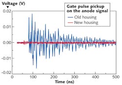
Fusion diagnostics
Laser fusion experiments are underway at the Laboratory for Laser Energetics (LLE; Rochester, NY), Laser Mégajoule (near Bordeaux, France), and the National Ignition Facility (NIF). The radiation emitted from the tritium targets at these facilities spans about 19 orders of magnitude in around 2 ns, so the diagnostics present many challenges.
Vladimir Glebov at LLE was the first to use a Photek double-MCP-PMT (with a gain of 106) to cover the early stages of the experiment, together with a single-MCP-PMT (with a gain of 5 × 10³) for the mid ranges and a photodiode with no gain at all to follow the final stages. NIF is currently using small, fast Photek PMTs with a 10-mm-diameter working area in the Gamma Reaction History (GRH) diagnostic, while the slower, larger 40-mm-diameter PMTs are being used in neutron time-of-flight (nTOF).
The application of PMT gating becomes particularly useful for nTOF diagnostics, where it is sometimes necessary to measure a small signal of "down-scattered" neutrons after a very large deuterium-tritium (DT) or hard x-ray signal, or to measure the neutron yield after a gamma flash in fast ignition experiments.2 The ability to gate the PMT between these close-proximity events prevents detector saturation (see Fig. 3). Two driving pulses were injected into an LED to simulate the main pulse and the down-scattered fraction (DSF). The main pulse was then removed to show the DSF by itself, and then the main pulse was restored but effectively ignored by the detector by gating out that time period. This shows how gating provides the ability to pick out small signals very close to large events. The area ratio of the main pulse to the DSF was 1000:1.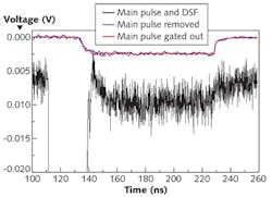
Particle accelerator applications
Future particle physics experiments are likely to use MCP-PMTs to improve time and spatial resolution (see Fig. 4). It is unlikely that higher-energy colliders will be built in the foreseeable future, but improved detectors are planned. For example, at the KEK High Energy Accelerator Research Organization facility (Tsukuba, Japan), MCP photomultipliers have been chosen for the detector upgrade.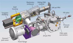
There are problems with the operational lifetime of MCPs, and Hamamatsu (Hamamatsu City, Japan) has improved life by inserting a very thin film approximately 8 nm thick between the photocathode and the MCP. In the US, the Large Area Picosecond Photo Detector (LAPPD) project aims to extend the operating life using completely new technology for the MCP. Instead of the traditional lead glass and hydrogen reduction, this project will use atomic-layer deposition to create the resistive and secondary electron-emitting layers.
High-energy particle accelerators often use Cherenkov radiation to detect the sub-atomic particles. The Cherenkov detectors generate extremely short light pulses containing many photons that effectively arrive at the PMT simultaneously. The presence of multiple photons in an event reduces the jitter of the time measurement even further. Experiments at Fermilab (Batavia, IL) have shown that the jitter of Photek MCP-PMTs can be as little as 7.7 ps for multiphoton events.
A key functionality required by particle accelerators is to have multiple parallel channels-often what is important is the detection of simultaneous multiphoton events at opposite sides of the collision point. Photek has collaborated with CERN (Geneva, Switzerland) and the University of Leicester (Leicester, England) to make multiple anode structures for MCP-PMTs to allow readout of simultaneous events and provide spatial information. This technology uses thin films printed onto a multilayer ceramic. An MCP-PMT with an 8 × 8 readout and an anode pitch of 1.6 mm (known as Hi-Content) has already been produced, and a 32 × 32 version with an anode pitch of 0.88 mm is about to be manufactured.
REFERENCES
1. Hirsch et al., Rev. Sci. Inst., 58, 12, 2339–2341 (1987).
2. www.lle.rochester.edu/media/publications/presentations/documents/APS09/Glebov_APS09.pdf.
Jon Howorth is director, James Milnes is R&D manager, and Gareth Jones is managing director at Photek, 26 Castleham Road, St. Leonards on Sea, East Sussex, TN38 9NS, England; e-mail: [email protected]; www.photek.co.uk.