UV OPTICS: Calcium fluoride micro-optics improve DUV excimer laser systems
UWE WIELSCH, KURT KANZLER, and TIM LINDSEY
In the world of ultraviolet (UV) photonics, system engineers are looking to micro-optics to solve some complex problems in the industry. Micro-optic components or array optics such as diffractive optical elements (DOEs), microlens arrays (MLAs), or more general refractive optical elements (ROEs) as well as hybrids of those, are enablers for many applications such as beam shaping for materials processing and pattern generation for illumination and semiconductor metrology.
Material choice is a critical decision for any photonics application. When lasers are involved the material specification can be the most important decision driving system lifetime, stability, and finally, cost. The rule of thumb is that shorter wavelengths demand more specialized materials and calcium fluoride (CaF2) is one of the best materials across the spectrum. Despite the fact that CaF2 is known to be a rather difficult material to machine or mold, state-of-the-art processing technologies for CaF2 do exist.
CaF2 material propertiesCalcium fluoride has much to offer. Besides being highly transparent in the DUV region, it also has excellent lifetime stability and relatively high damage threshold in the DUV, making it the material of choice for excimer systems at these wavelengths. Furthermore, CaF2 has a broad transmission range, from 140 nm to 7.5 µm and beyond. Calcium fluoride also is inert to organic chemicals and many acids—including hydrofluoric acid—and can be used up to 1000ºC in dry environments.
With its relatively low index of refraction (1.5016 at 193 nm and 1.4680 at 248 nm), CaF2 can be used in some 193 nm applications without any thin-film coatings. However, if thin-film coatings are applied, the coating material choice and process will define the lifetime of the optic. The choice of oxide- or fluoride-based coating materials can change the performance for challenging 193 nm CaF2 applications.
Stress is another property that should be considered. Due to the crystalline nature of CaF2, unequal stresses in its crystal planes can increase birefringence or even cause the part to fracture or break during processing. Hence any steps that could increase stresses in the material must be avoided during fabrication.
Manufacturing CaF2 micro-opticsMore than 10 years ago, micro-optics were introduced into 355 nm laser material-processing applications like via drilling and precision machining. These components are typically fabricated from fused silica or crystalline quartz and the transmission window for these materials is sufficient for many applications at longer UV wavelengths. However, as lasers have become more efficient with higher output powers, more suitable materials are needed.
Up to now fused silica was the material of choice for almost all DUV applications, although it does degrade over time in high-end (or high-power) UV applications. The process of compaction or micro-channeling in fused silica changes the density and index of refraction of the bulk material over time as it is exposed to higher UV energy at 193 nm. The change of refractive index then alters the wavefront properties for transmissive fused-silica optics. Fortunately, CaF2 does not show this behavior. However, fabricating these diffractive and refractive microstructures in CaF2 has been difficult with existing technology and has been limited to cylindrical cross-sections or linear geometries.
Traditional fabrication techniques for manufacturing CaF2 optics are single-point diamond turning (SPDT) and optical polishing. These techniques have also been applied to the fabrication of micro-optics. However, a non-traditional etching technique is becoming readily available to fabricate diffractive and refractive micro-optics.
Using wafer-scale fabrication, it is now possible to create refractive homogenizers that are not only cylindrical (or acylindrical), but also square and rectangular in profile (see Fig. 1). With this capability, very sharp homogenized profiles can be realized in only two surfaces—where four surfaces or more were needed in the past. Also, system engineers can now correct for astigmatism effects in fewer surfaces than before. Typical wafer geometries can be 100 or 150 mm in diameter, with thicknesses in the 1–4 mm range.
But micro-optics fabricated from CaF2 are not limited to refractive structures. It is also possible to create diffractive profiles in CaF2 with efficiencies >90% with very flexible illumination patterns (see Fig. 2). Whether the requirement is for mask or wafer-defect inspection, it is possible to create uniform illumination or Gaussian illumination using flexible patterns other than square or rectangular profiles. Using grayscale photolithography, diffractive-optic efficiencies can be very high and speckle can be reduced.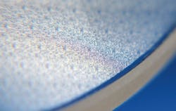
UV applications
Applications in the semiconductor and biomedical industries are pushing development of deep-ultraviolet (DUV) laser systems and the accompanying optics and optical materials. Frontend lithography tools working at 193 nm are using double-patterning techniques for current and future nodes that require the lithography tools to perform at twice the speed. Double-patterning delivers very small features, which in turn drives the very tough requirement of measuring and inspection of these features, which includes (but is not limited to) measurement of reticle defects, reticle critical dimensions, the prediction of the reticle (and defect) printability, measurement of overlay accuracy, and wafer inspection (patterned and bare wafer). In these areas there is a trend toward shorter wavelengths to enhance resolution and follow the smaller feature sizes.
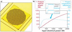
Higher-power excimer lasers and more efficient optics and micro-optics can help to get more light through the system, satisfying the need for higher throughput and extending the lifetime of these DUV systems.
Lasers are also replacing mechanical tools in material-processing applications such as cutting, micromachining, UV curing, ablation, and annealing. Performance of laser material-processing equipment is often increased by micro-optical components including diffractive and refractive beam shapers, diffractive beamsplitters, line-beam generators, and homogenizers. In these instances, CaF2 is a favorable material for increasing laser power at the workpiece—particularly in the UV.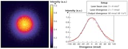
But DUV laser systems are not limited to the semiconductor and material-processing industries. In the health care and life sciences markets, for instance, DUV excimer laser systems are used in ophthalmology to help shape the human cornea for correction of myopia, hyperopia, and astigmatism. For these demanding applications, it is important to homogenize light and/or create Gaussian profiles from a non-Gaussian laser source. Micro-optics technology is the primary choice for these applications, and CaF2 etched micro-optics are meeting these application demands (see Fig. 3).
Uwe Wielsch is head of sales, micro-optics, at Jenoptik Optical Systems GmbH, Goeschwitzer Strasse 25, Jena, Germany 07745. Kurt Kanzler is in business development, micro-optics–West Coast, and Tim Lindsey is sales manager, Jenoptik Optical Systems Inc., 1 Industrial Parkway, Easthampton, MA 01027; e-mail: [email protected]; www.jenoptik.com.