ULTRAFAST LASERS: High-power pico- and femtosecond lasers enable new applications
SASCHA WEILER
The industrial implementation of cold laser ablation, cutting, and drilling by use of ultrashort pulses has been a vision for more than 20 years. Early experiments with Ti:sapphire amplifiers as the paradigm of ultrafast technology during the last decades have demonstrated the huge potential of ultrashort laser pulses for precision machining. But how short is short enough for precision machining? What happens when a laser pulse hits material and on which timescales?
Principles, timescales, energy density
The absorption of a laser pulse in metals, for example, is basically an energy transfer from the laser pulse to the electrons of the material. For nanosecond pulse durations a temperature equalization between electrons and lattice sets in (which is heating), and finally begins melting the material until partially evaporating it.
The shorter the pulses, the faster the energy transfer to the electrons. Ideally the pulses are so short that there is not enough time for temperature equalization of electrons and lattice. Then the “hot electrons” (in contrast to the cold lattice) have two ways to couple with the lattice: After a characteristic time, heat diffusion from the electrons to the surrounding lattice begins. This electron-phonon-relaxation-time is a material property and has a typical value on the order of 1–10 ps. At approximately the same timescale, but a bit delayed, an abrupt energy transfer between the hot electrons and the lattice takes place, resulting in a phase explosion, i.e., evaporation of the excited volume.
From these explanations, two fundamental conclusions can be drawn:
1. The duration of the laser pulse must be short enough to prevent temperature equalization between electrons and lattice. For metals and most other materials, this demands pulse durations of 1–10 ps or less.
2. As there is a time delay between heat diffusion and ablation there is always residual heat, even for the shortest pulses.
Cold processing must therefore be defined as processing with minimal heat diffusion, which requires pulse durations of 1–10 ps or less.
While pico- or femtosecond pulse duration is a necessity for cold processing, it is not sufficient. If the hot electrons get over heated by applying a too-high energy density, then heat diffusion effects become visible, which turn the process to be thermal. As a rule of thumb, energy densities around 1 J/cm2 are the sweet spot for ablation with pico- and femtosecond pulses without measurable heat effect, i.e., low thermal penetration depth.
Linear vs. nonlinear absorption
Unfortunately, nature did not make it that easy. Besides the aforementioned factors that determine the thermal impact, there is also the optical penetration depth—determining which fraction of the laser pulse gets absorbed in what depth.
For gentle ablation, the optical penetration depth should be in the area of 1 µm or less. There are three main reasons for this:
1. The optical penetration depth determines the depth of ablation. Too-high depths of ablation are no longer considered as gentle ablation, as the result is rough surfaces and edges—and especially for hard and brittle materials micro-cracks are induced.
2. The ablation process becomes inefficient, as most of the laser pulse might not be absorbed and is therefore wasted.
3. Especially for selectively ablating material from a carrier (e.g., patterning of thin films on insulators like thin-film solar cells), the transmitted light might cause damage to the carrier material.
The influence of the linear absorption of femto- and picosecond pulses is often neglected with the statement that the pulse’s peak powers are so high that nonlinear absorption through multiphoton processes becomes dominant to linear absorption. If the described boundary conditions for pulse duration and energy density are met, then this statement is often misleading.
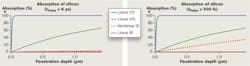
To visualize this, the absorption curves for silicon are plotted for an energy density of 1 J/cm2 (see Fig. 1). For pulse durations of 6 ps and longer, the linear absorption is absolutely dominant above the nonlinear absorption. Even going to 500 fs does not change the situation: The nonlinear absorption is still far too low to reach the desired 1-µm-scale optical penetration depth.
Choosing an ultraviolet wavelength results in the theoretically best performance as well as in praxis (e.g., for dicing silicon wafers). For some purposes, a green wavelength might lead to sufficient results in processing silicon, but infrared wavelengths fall under points 1–3.
Femtosecond as well as picosecond pulses with proper energy density and wavelength are suitable for processing materials where thermal influence must be minimized. Furthermore, for picosecond pulse durations, the technical approach to generating these pulses can be greatly simplified. Direct diode pumping and amplification (power scaling) without chirped-pulse amplification (CPA) are necessary requirements for the success of ultrashort pulse technology in the industrial market. Added to this is the fact that for a cost-effective application in industrial micro-processing, scaling the average output to values of 50 W and greater is necessary.
Productivity through power scaling
Since the 1970s, rod-type lasers—first lamp-pumped and later diode-pumped—have been produced. While pushing the beam-quality limits of high-average-power, rod-type lasers, diode-pumped disk laser technology was developed in the 1990s to become the industry’s most reliable technology for kilowatt CW operation.
Both fiber laser and disk laser technology are superior to conventional rod-type lasers in using a larger cooling surface compared to the laser-active volume, enabling TEM00 CW operation at power levels up to 500 W and more. At equal brilliance, however, the small fiber core causes the intensity inside a fiber laser to be dramatically higher compared to a disk laser.
However, when amplifying picosecond and femtosecond pulses, high intensities result in nonlinear effects such as self-phase-modulation or Raman scattering, requiring sophisticated chirped-pulse-amplification in ultrafast fiber amplifiers or limiting the maximum achievable pulse energy to values of 6 µJ or below. Using disk laser technology as the amplifier for picosecond pulses enables high peak power (up to 100 MW) with low intensities and therefore no nonlinearities.
Combining fiber and disk
To realize a picosecond laser with high pulse energies (up to 250 µJ) and high average powers (up to 100 W) a master oscillator power amplifier with the following unique configuration is used: A passively modelocked fiber laser based on telecom components acts as a monolithically integrated, cost-effective, and reliable source for low-power and low-pulse-energy picosecond pulses.
Using the capabilities of the disk laser enables amplification by more than five orders of magnitude to power levels of more than 100 W infrared and 60 W in green, and pulse frequencies from 200 to 800 kHz, with no need to use sophisticated chirped-pulse amplification. Even at these power levels, excellent beam quality, represented by guaranteed M2 values of <1.3, is achieved. Furthermore, the output beam quality is staying at the above-stated values for every selectable parameter combination of the laser.
Power to the workpiece
Behind the laser exit window, the main task is to manipulate the laser beam and transfer the laser power to maximum productivity and quality. Balancing part and feature geometry with accuracy requirements results in an equation with many unknown aspects. Solving this equation requires a kit of optical components, such as scanners, F-Theta lenses, focus optics with coaxial gas nozzle, waveplates, trepanning optics, and many others.
These need to be combined with linear or rotary stages for high-precision or tubular part geometry. Neither state-of-the-art linear stages nor scanners have the dynamics to apply pulse frequencies of more than 1 MHz, although laser technology may be ready for this development.
Drilling applications
Producing fuel-saving, low-emissive engines is a major challenge for the automotive industry, and the key to solving this problem is cleaner burning of the fuel. This can be accomplished by optimizing the nozzles for fuel injection.
Drilling an injection nozzle hole with a high-power picosecond laser produces very sharp edges with no burr or melt and low surface roughness inside the hole, resulting in an optimum spray cloud of the fuel. Furthermore, the taper of the hole can be varied from positive over zero (parallel) to negative values, giving another degree of freedom to optimize the injection process. The combination of 50 W average power, together with a pulse energy as high as 250 µJ, enables drilling of these high-quality holes with unmatched throughput (see Fig. 2).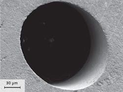
Cutting semiconductor wafers
The current, state-of-the-art singulation of computer chips from a silicon wafer is dicing by diamond blade saws. The silicon wafer is typically mounted on a die-attached tape—a sticky tape in a metal frame that fixes the wafer. The separated dies can then be picked and placed into lead-frame packages. However, thin silicon wafers become flexible and a challenge for blade saw dicing machines. Because of the mechanical contact, wafer saws must operate very carefully to avoid breaking the die or producing chips along the cutting edge.
Picosecond lasers in combination with high-speed and precision linear stages can be used as a noncontact tool to produce die-singulation results faster than a blade saw. A further advantage of using picosecond pulsed lasers is the high cutting quality and the negligible heat-affected zone. This leads to cutting edges with high strength, which is essential for the die to sustain mechanical load during the next processing steps (see Fig. 3).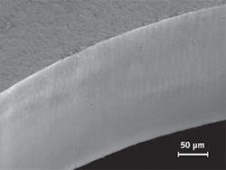
Cutting cardiovascular stents
Stent manufacturers are trying to take advantage of polymeric materials, such as those that are bioresorbable. State-of-the-art laser fusion cutting with CW fiber or solid-state lasers can only be applied to metal stents and produces melt and burr, which require expensive post-processing and reduce yield.
With the proper selection of wavelength, cutting optics, and rotary stage, picosecond lasers can compete with the speed of fusion cutting and give a distinct advantage in cutting quality, which reduces the amount of post-processing to a minimum and results in higher yield. In addition, the same picosecond laser can be used to cut polymer and other nonmetallic stents with high speed and quality, making it a potentially disruptive and universal tool for medical device manufacturing (see Fig. 4).
Cutting display glass
Display manufacturers are looking for cutting solutions where the resulting glass exhibits an edge with high strength. In addition, industry trends are leading to ultrathin glass for OLED displays and chemically hardened cover glass on the material side, and a demand for flexible shapes for fancy designs.
Similar to silicon, glass is a brittle-rigid material. State-of-the-art cutting of display glass is done by mechanical scribing and breaking along the straight scribe. The resulting cut edges typically exhibit cracks and chipping and a poor edge strength, which makes grinding an unavoidable post-processing step. The necessity of grinding not only limits the flexibility in lateral geometry but also in glass thickness.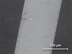
Years of application development have led to a breakthrough for picosecond lasers in mass production of mobile displays (see Fig. 5). Not only in terms of edge quality but also for flexible (nonlinear) geometries, picosecond lasers have proven to be versatile tool, with the ability to cut ultrathin to hardened glass.
Sascha Weiler, PhD, is program manager, micro processing, with TRUMPF, Farmington, CT; e-mail: [email protected]; www.trumpf.com.