MICROELECTRONICS PROCESSING: 'Zero-overlap' laser system speeds ultrathin wafer dicing
Solid-state, fiber-based, and ultrafast lasers continue to make inroads in microelectronics processing applications, specifically for silicon wafer dicing in the semiconductor industry and in a variety of laser-based cutting and texturizing applications in the photovoltaics industry.
While most of these laser-based cutting methods rely on linear movement of the laser beam along a substrate, Electro Scientific Industries (ESI; Portland, OR) has developed a production-ready system that incorporates its new laser-based "zero-overlap" technique for dicing ultrathin (less than 50 μm thick) silicon wafers. By keeping pulse energies and repetition rates high, yet separating the pulses spatially along the scribe line, ESI says its turnkey system improves throughput, yield, and die-break strength of ultrathin wafers compared to linear laser-based dicing methods or conventional mechanical sawing methods.
Ultrathin wafer challenges
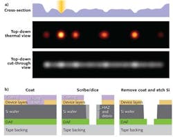
The unstoppable progression of Moore's law is driving the semiconductor industry toward 3D integration and such advanced packaging architectures as stacked memory and logic, as well as through-silicon-via (TSV) interconnects. As wafers move to thinner form factors, mechanical wafer-dicing techniques fall short due to cracking, chipping, and other yield and quality issues. The ESI 9900 enables full-cut dicing of ultrathin wafers and scribing logic or system-on-chip (SoC) wafers on die-attach films (DAFs) in one integrated system. Because these wafers often have delicate, brittle, low-κ dielectric materials on the topmost layers of the wafer, cutting through these layers without damage is critical.
The 'zero-overlap' technique
The 9900 zero-overlap technique uses a galvanometer-based positioning system to rapidly distribute the thermal energy from a 355 nm commercially available UV laser (with approximate 8 μm spot size) to spatially separated points along the desired scribe line of a wafer. Pulsing at around 240 kHz, the laser energy is delivered in multiple passes in spatially separate pulses that avoid the debris, heat buildup, and plume interactions of linear laser-based scribing methods. The spatial separation allows the use of higher laser-fluence values for higher wafer-cutting speeds (a few meters per second) than would be possible using linear movement of the laser beam. In addition, the laser pattern can be selectively optimized to control material removal rates for different semiconductor layers (see figure).
"The system singulates the top device layer, through the silicon, and then through the DAF with robotic wafer handling, dry etch, and cleaning steps in one fully automated process," says Matthew Knowles, product marketing manager at ESI.
Even though ESI has shown that this technique minimizes the heat-affected zone (HAZ) of the substrate being processed, they admit that any laser-based process is a thermal process and some HAZ exists. To maximize die strength and minimize kerf width of the cut, the zero-overlap process is followed by a conventional dry etch. Currently, ESI can produce clean cuts with a 20 μm kerf width after the laser cut and etch process. The 9900 also has software that includes customer-specific recipes of laser dicing parameters unique to the materials being processed.
"We are currently working with customers to optimize the laser and etch processes and are encouraged by the high die break strengths and high production yields we are seeing," says David Lord, product manager in ESI's Semiconductor Products Division. "Our goal is to minimize cost of ownership for the customer and enable our customers to fully adopt 3D integration into their high-volume manufacturing environments."
About the Author

Gail Overton
Senior Editor (2004-2020)
Gail has more than 30 years of engineering, marketing, product management, and editorial experience in the photonics and optical communications industry. Before joining the staff at Laser Focus World in 2004, she held many product management and product marketing roles in the fiber-optics industry, most notably at Hughes (El Segundo, CA), GTE Labs (Waltham, MA), Corning (Corning, NY), Photon Kinetics (Beaverton, OR), and Newport Corporation (Irvine, CA). During her marketing career, Gail published articles in WDM Solutions and Sensors magazine and traveled internationally to conduct product and sales training. Gail received her BS degree in physics, with an emphasis in optics, from San Diego State University in San Diego, CA in May 1986.