PHOTONIC FRONTIERS: NEXT-GENERATION PHOTOVOLTAICS: New techniques boost photovoltaic efficiency

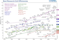
The bright promise of clean, green electricity has lured investors and governments into major investments in photovoltaic technology and production. Solar cell efficiency in converting light energy into electric power has increased steadily over the past 35 years (see Fig. 1). However, that progress seems modest compared to semiconductor electronics. The computer on your desk can run rings around the state-of-the-art in 1977–an Apple II with a 1 MHz processor and 4 Kbyte of RAM. Yet during those 33 years, power conversion efficiency of single-crystal silicon solar cells has barely doubled, from around 13% in 1977 to nearly 28% today.
Now developers hope they can push photovoltaic performance to much higher levels in new generations of solar cells. Their goals are not to find new photovoltaic materials but to use new techniques to enhance the efficiency of established materials. One goal is to refine the internal structures of inorganic thin-film semiconductors, which can be deposited as thin films on inexpensive substrates to make low-cost, large-area solar cells. Another goal is to build internal micro- and nanostructures that improve the efficiency of light collection, conversion, and power generation. Other efforts were covered in our June issue (see Laser Focus World, p. 59, June 2010).
Doubling CdTe efficiency
Thin-film technologies based on inorganic semiconductors have gained favor for large-area solar generation facilities because they can be deposited on inexpensive substrates such as glass, thereby greatly reducing the material costs of panels.
The most widely used thin-film material is cadmium telluride (CdTe). The National Renewable Energy Laboratory (Golden, CO) has achieved efficiencies of 16.7% in small CdTe solar cells in the laboratory, but that requires expensive substrates. The best efficiency achieved for CdTe on glass is 13.8%, says W.S. Sampath of Colorado State University (Fort Collins, CO). Scribing the glass and adding the electronic circuits needed to connect individual solar cells in series reduces conversion efficiency to 10–11%.
In June, the National Science Foundation (NSF) awarded Colorado State a five-year, $450,000 grant to establish an industry/university cooperative research center for next-generation photovoltaics that Sampath will head. The university will team with five companies–Abound Solar (Loveland, CO), 5N Plus (St. Laurent, QC, Canada), Pilkington North America (Toledo, OH), Ion Edge Corp. (Fort Collins, CO), and MBI Corp. (Ft. Collins, CO)–each of which will contribute a total of $400,000 over the coming five years. The goal, says Sampath, "is to go to 20%, or possibly 30% conversion efficiency" in commercial devices.
Now produced in high volume at low cost by First Solar (Tempe, AZ), current-generation CdTe photovoltaics are single-junction devices, with layers of binary cadmium sulfide and CdTe deposited on 2 × 4 ft slabs of passivated window glass. "We want to keep all the present advantages in manufacturing and go into more complex alloys and materials" to improve performance, says Sampath.
Sampath says the project will look at multijunction structures, including ternary and quaternary compounds. The researchers are investigating cadmium zinc telluride (CdZnTe) and cadmium magnesium telluride (CdMgTe) for short wavelengths and other compounds for longer wavelengths. Challenges include passivating boundaries between materials and fabricating additional junctions without damaging the bottom layer.
Ink-jet printing thin films
Brian Korgel of the University of Texas at Austin also is working with the NSF consortium to improve performance of other thin-film materials including copper-indium-gallium selenide (CIGS). Laboratory efficiency has reached 20%, but CIGS is not as well developed commercially as CdTe.
Korgel is developing inorganic semiconductor "inks" that can be printed onto inexpensive substrates. "We like CIGS," he says, because 30 years of research have identified only it and CdTe as viable alternatives to silicon for solar cells, but he's also exploring other possibilities. Printable materials would avoid the need for the high-vacuum and high-temperature processing needed for vapor-phase deposition, and could allow printing on flexible materials like plastics. That could reduce the costs of manufacturing solar cells by a factor of 10, a huge drop that may lead to new applications.
Nanostructures: Pillars and coax
Other groups are looking at more drastic redesigns of solar cells to control light absorption and current generation better than is possible in conventional planar solar cells. A fundamental problem is balancing the requirements for light absorption and current conduction. Light absorption increases with the distance the light travels through the semiconductor, but the thicker the semiconductor layer, the more energy electrons lose in passing through it. So developers are exploring ways to make the light and the current carriers follow different paths through the material.
One approach is fabricating regularly spaced arrays of semiconductor nanopillars on the surface. Light passing vertically along the pillars would generate current carriers that could be conducted horizontally to the sides of the pillars, where they could be transferred to a more conductive material, such as a transparent conducting layer on the surface. An alternative demonstrated last year by Ali Javey and colleagues at the University of California at Berkeley (Berkeley, CA) is to fabricate nanopillars of single-crystal CdS, then surround them with polycrystalline CdTe. The CdTe absorbs most of the light, with the CdS pillars serving as conductors for the electrons.1
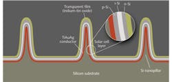
Better conductivity is possible by fabricating "nano-coax" on the surface instead of simple pillars, says Michael Naughton of Boston College (Newton, MA). The structure is formed by depositing a series of layers on a silicon substrate with nanopillars rising from its surface (see Fig. 2). Working with Kris Kempa and Shifeng Ren of Boston College, Naughton coated the nanopillars with a thin metallic conductive layer, then deposited successive layers of p-doped, intrinsic, and n-doped amorphous silicon to form a thin-film solar cell coating on the nanopillars. Coating that structure with a transparent conductor produces the nano-coax.The conductors could act as optical antennae to absorb light incident vertically on the surface, but the silicon layer absorbs it first, generating holes and electrons that travel horizontally. The junction generates an electric field, separating the carriers so holes go to one conductive layer and electrons to the other. The conductors then go to the top or bottom of the nano-coax layer, producing a photovoltage. This separation of the light and carriers produces a thick vertical layer that absorbs the light efficiently but thin horizontal layers that conduct current efficiently. Naughton initially achieved 9% energy-conversion efficiency.2 In an interview, he says NREL has now certified 10.5% efficiency, approaching the 12.5% record for amorphous silicon.
Hot electron transfer
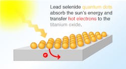
Separating light and current carriers is only one of three steps needed to restructure solar cells for much better efficiency and create a third (new) generation of highly efficient solar cells, Naughton says. Developers also need to capture all the energy of the incoming photon, not just the bandgap energy. Incoming photons actually do transfer all their energy to the electron they excite to the valence band, but normally it loses all that excess energy in less than a picosecond as phonons that excite vibrations within the semiconductor. Last year, Naughton showed that some of these photons could be extracted from an extremely thin solar cell, but light absorption was too low to be practical.3 In June, Xiaoyang Zhu's group at the University of Texas at Austin found a better approach to trapping hot electrons.4 They used lead selenide quantum dots, in which electron energy levels are separated by an energy much larger than the highest phonon energy. This creates a "phonon bottleneck," which keeps the hot electron from losing energy in single-phonon increments. That allowed the hot electrons from the PbSe quantum dots to be transferred to an adjacent titanium dioxide layer in less than 50 fs (see Fig. 3).Extracting all the energy from hot carriers could raise solar cell efficiency to 66%, Zhu's group writes, more than double the record for any single-junction cell. "It's great work, but it's not a solar cell," says Naughton. Hot-electron extraction would have to be combined with separating paths of the light and current carriers, and the whole thing has to be packaged into a solar cell and connected to electrical conductors in a way that doesn't dissipate the energy of the hot carriers in the wires. Nobody expects that to be easy, but the new experiments make it look plausible.
Outlook
Successful laboratory demonstrations will only be an early step on the road to a practical next generation of solar cells. The technology must be made affordable, and cost-performance tradeoffs will have to be worked out both for manufacturing and deployment. Today's most efficient solar cells are the most expensive to make per square centimeter and often require solar concentrators for best performance. The solar future won't come easily. But we can see encouraging signs that it is coming.
REFERENCES
1. Z. Fan et al., "Three-dimensional nanopillar-array photovoltaics on low-cost and flexible substrates," Nature Materials 8, 648–653 (2009); doi: 10.1038/NMAT2493.
2. M. Naughton et al., "Efficient nanocoax-based solar cells," Phys. Status Solidi Rapid Res. Lett. 4, 181–183 (2010); doi: 10.1002/pssr201004154.
3. K. Kempa et al., "Hot electron effect in nanoscopically thin photovoltaic junctions," Appl. Phys. Lett. 95, 233121 (2009).
4. W.A. Tisdale et al., "Hot electron transfer from semiconductor nanocrystals," Science 328, 1543–1547 (June 18, 2010).
About the Author
Jeff Hecht
Contributing Editor
Jeff Hecht is a regular contributing editor to Laser Focus World and has been covering the laser industry for 35 years. A prolific book author, Jeff's published works include “Understanding Fiber Optics,” “Understanding Lasers,” “The Laser Guidebook,” and “Beam Weapons: The Next Arms Race.” He also has written books on the histories of lasers and fiber optics, including “City of Light: The Story of Fiber Optics,” and “Beam: The Race to Make the Laser.” Find out more at jeffhecht.com.


