METAMATERIALS: Electromagnetic 'black hole' is experimentally realized
The subwavelength structure of optical metamaterials gives them their unique properties—and also makes them challenging to fabricate. This is why metamaterials researchers sometimes first opt to put their ideas into practice in the microwave region, which brings the size of a structure's unit cell up from a few hundred nanometers to a few millimeters. Once proven with microwaves, the concept can then (at least sometimes) be scaled down into the optical regime.
Researchers at Southeast University (Nanjing, China) have taken an idea first proposed last year and implemented it in the microwave region.1 The idea—a metamaterial omnidirectional optical absorber, or electromagnetic "black hole"—was first proposed last year; if ultimately created in the optical region, the device could be useful for maximizing the light absorption of solar cells and photodetectors.2
Radially varying permittivity
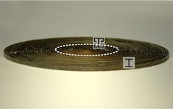
The experimental microwave device is 2D for simplicity (see Fig. 1). Its overall effect is that of a dielectric cylinder with a lossy inner core and a lossless circular shell with a permittivity that varies with radius. All electromagnetic waves of any polarization at the design frequency that hit the cylinder, even at a glancing angle, are captured and spiral inward to the core.
As in many microwave metamaterial structures, the unit cells consist of pieces of circuit-board material with specific metal shapes etched onto them. To create a radially varying permittivity, the metal shapes are changed as a function of radius. For example, the shapes could be circular rings, "I" shapes, or Jerusalem crosses; the dimensions of the individual shapes can be varied as well. The researchers chose a non-resonant I shape for the outer shell of the absorber, and an electric-field-coupled (ELC) resonator for the inner core.
A microwave frequency of 18 GHz was chosen for the experiments. The unit cells were 1.8 mm in size, or about 1/10 the wavelength of the radiation to be captured; the entire device had 60 concentric layers, with all layers three cells high. To fix the layers in place, circular slots were cut into a styrofoam board and the layers fit into the slots.
Dark shadows
In the experiment, a nearfield scanning system measured the incident microwaves and what happened to them as they entered the absorber; the scanning system could measure a 400 mm2 area to a resolution of 0.5 mm (the absorber itself was 216 mm in diameter). For comparison, specialized numerical software was used to simulate the absorber and its ability to capture microwaves.
The absorption of a simulated Gaussian beam striking the absorber at normal and off-center incidences was calculated to be 99.94% and 98.72%, respectively. Experimentally, it is difficult to create a small Gaussian microwave beam, so an easier-to-generate beam was used for the experiment. The path and behavior of the beam, which was narrow but slightly divergent, was mapped and shown to be similar in behavior to simulations; in both, the beam is seen to enter the absorber and spiral toward the core.Additional simulations of the response of the absorber to a plane wave were made for the distributions of both the electric field and the power (see Fig. 2). A simulation of the behavior of the absorber when subjected to an electric field radiated by a nearby monopole source agreed well with the experimental measurements of the same arrangement; both showed a shadow region cast by the absorber.
The researchers believe that, because the core of the device absorbs radiation and emits it as heat, the omnidirectional absorber could find use as a thermal emitter or a "harvester" of electromagnetic radiation.
REFERENCES
- Q. Cheng et al., New J. Phys. 12, 063006 (2010).
- E.E. Narimanova and A.V. Kildishev, Appl. Phys. Lett. 95, 041106 (2009).
About the Author
John Wallace
Senior Technical Editor (1998-2022)
John Wallace was with Laser Focus World for nearly 25 years, retiring in late June 2022. He obtained a bachelor's degree in mechanical engineering and physics at Rutgers University and a master's in optical engineering at the University of Rochester. Before becoming an editor, John worked as an engineer at RCA, Exxon, Eastman Kodak, and GCA Corporation.


