MINIATURIZED IMAGING SPECTROMETERS: Prism-based spectrometers tackle today's miniaturization requirements
JEREMY LERNER
It is truly said that form follows function; however, increased miniaturization inevitably collides with practical realities. Surprisingly, however, technologies over 300 years old are finally experiencing a rebirth in cutting-edge applications. Sir Isaac Newton first described the use of a prism to display the colors present in the sun's light in 1666. This promising beginning was soon usurped by the diffraction grating and by the late 1800s grating-based spectrometers became the de facto standard. But by the year 2000, grating-spectrometer development had more or less hit a plateau, failing to satisfy some of the more demanding and emerging applications that often require miniature spectrometers or microspectrometers in a handheld or portable format.
The remote-sensing community, for example, pioneered the use of hyperspectral imaging to correlate objects in a heterogeneous field of view (FOV) with their spectral characteristics. To satisfy the needs of this community, imaging spectrometers were developed that used prisms and prism-grating combinations (grisms). This new generation of imaging spectrometers has since been adapted to address complex applications including automated pathology, biomedical imaging, and nanoparticle imaging and characterization.1, 2
Imaging versus non-imaging spectrometers
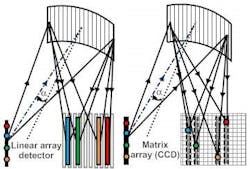
In the early 1900s it was observed that all spectrometers took a point and imaged it as a line, at each wavelength, on the detector. The image of a point on the entrance slit was not only elongated due to astigmatism but also suffered from curvature and other aberrations (see Fig. 1). This not only made it impossible to differentiate between the spectra presented by two adjacent objects, but also spread the light over a large area, reducing photon density and sensitivity.
A true imaging spectrometer images a point in the FOV as a point on a detector at each wavelength. With this capability it is possible to reconstruct the spectral characteristics of a heterogeneous FOV, which satisfies the imaging requirements of most applications.
Grating-based imaging spectrometers reduce astigmatism and other aberrations by using aspheric optics or gratings with asymmetrically distributed grooves (ADG) produced holographically, or with sophisticated ruling engines.3-6 The challenge is to produce a diffraction grating that possesses the optimum focal length, groove density, and wavelength efficiency, in a size that makes sense.
The quest for lighter, robust, more sensitive spectrometers that operate over extended wavelength ranges within the remote Earth-sensing community has resulted in the development of a new generation of prism-based, compact spectrometers.
Spectrometer basics
Whether a spectrometer uses a grating or a prism, all wavelength-dispersive spectrometers image an entrance slit onto a detector, at each wavelength. Unlike a classical spectrometer, an imaging spectrometer dissects the image of the entrance slit along its length (perpendicular to the wavelength dispersion axis). In use, an FOV is imaged onto the slit; then, all objects appearing along the slit present their spectra to the detector. To generate a spectral map, referred to as a hyperspectral image, the spectrometer is either flown over the FOV or the FOV is translated underneath the spectrometer on a conveyor belt or automated translation stage. In both cases the spectrometer is used as a spectrograph in which all wavelengths are acquired simultaneously at each location along the slit.
The ideal wavelength detector for an imaging spectrometer is a CCD camera where each row of pixels is assigned to a location on the entrance slit. Each row of pixels acquires a complete spectrum from each location and the spectrum of each point on the slit is dispersed across a specific row of pixels. The spatial resolution is limited by the height of a row of pixels and the spectral resolution is determined by the properties of the spectrometer, unless the CCD camera is mismatched to the spectrometer. After establishing the required spatial/spectral resolution and wavelength range of the application, the operating parameters of the instrument can be calculated.7, 8
Spectral and spatial resolution
Given that the entrance slit is imaged onto the detector bandpass, spectral resolution (or bandpass BP) is defined as BP = Sw * Wd. Here, Sw = image of the entrance slit (mm) and Wd = wavelength dispersion (nm/mm). The average wavelength dispersion, Wd, is the required wavelength range divided by the length of a row of pixels. If the application characterizes a field of nanoparticles then the wavelength range needs to stretch from 400 to 800 nm—a 400 nm spectral segment. And if each pixel in the CCD detector is 4.65 × 4.65 µm arrayed along rows 6.47 mm in length, then the average Wd will be 400 divided by 6.47 mm, or 62 nm/mm.
Assuming the application demands a spectral resolution of better than 2 nm (and for expediency it would be desirable to use is a standard 25 µm slit width), then the system bandpass will be 0.025 × 62, or 1.55 nm. Actual values of Wd and Sw vary with wavelength, so spectral resolution will vary across the spectral range.
The image of the entrance slit will present a full width at half maximum (FWHM) of approximately 25 µm (Sw) and will occupy an integer number of pixels, with the number of pixels defining the FWHM as 25/4.65 or 6.
Only three pixels are required to accurately determine the peak wavelength and the half maximum points; therefore, there would be no loss in spectral resolution and a gain in sensitivity if rows of pixels were binned two by two. This condition satisfies the Raleigh criterion for spectral resolution when the FWHM is that of the entrance slit when illuminated by a monochromatic wavelength such as a single-mode laser or a low-pressure mercury discharge lamp. It is worth emphasizing that spectral resolution depends on the width of the image of the entrance slit, not the total number of pixels on the CCD chip.
A spectrometer's spatial resolution is determined by the convolution of residual spectrometer aberration and the height of a row of pixels. The net spatial resolution is a quadratic where spatial resolution equals the root of the sum of the squares of residual system aberrations, the size of a pixel, and any other contributing factors.
A minimum of at least two pixels are required to determine the location of an object on the entrance slit; therefore, if the FOV is imaged with a 40X microscope objective the spatial resolution at the FOV would be approximately 0.45 µm.
Correcting aberrations in a prism-based spectrometer
Diffraction-grating spectrometers enable aberration correction through modified groove distribution or the use of aspheric focusing or collimating optics. The use of aspheric optics with a prism is feasible, but unnecessary if the prism itself can be given "power" (see Fig. 2). This special power geometry used optics with curved sides, and was originally developed for the SEBASS remote hyperspectral imaging system (www.lpi.usra.edu/science/kirk land/home.html) that is flown on aircraft and operated in the far-infrared spectrum. A redesign for use in the wavelength range from 365 to 920 nm resulted in LightForm's PARISS hyperspectral imaging system (www.pariss-hyperspectral-imaging.com) for use mounted on any microscope for biomedical, forensic, and industrial spectral imaging.9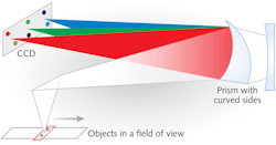
The optical system comprises a prism with one side concave, the other convex, and a spherical mirror for focusing. The effective wavelength dispersion is doubled because light passes through the prism twice. Ray tracing is used to determine the optimum curves of the mirror and prism faces and the distances between the mirror and prism.
Grating- versus prism-based spectrometers
Diffraction-grating efficiency varies considerably with wavelength and peaks at the blaze wavelength (see Fig. 3). If a grating is non-blazed, such as many holographic gratings, the peak efficiency is lower but can extend over a longer wavelength range.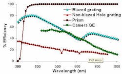
In comparison a prism has a flat 90% transmission efficiency over a very wide wavelength range. This makes it feasible to use significantly less expensive cameras with lower quantum efficiency (QE). The majority of wavelength-sensitive detectors (including photomultiplier tubes, CCDs, and most silicon-based detectors) have QE profiles that are very similar to the efficiency profiles of blazed diffraction gratings.
For both a prism and a typical diffraction grating, wavelength dispersion is nonlinear. But because the nonlinearity is greatest for a prism, there is a surprising benefit: Given that spectral resolution and bandpass are a function of wavelength dispersion, a decrease in wavelength dispersion to longer wavelengths results in a decrease in spectral resolution. Therefore, the spectral resolution of prism spectrometers is greatest in the blue and lowest in the red. However, light throughput is directly proportional to bandpass. This is an advantage when working with weakly emitting samples because as the QE of the camera decreases, the light throughput of a prism increases as a function of its bandpass (see Fig. 4).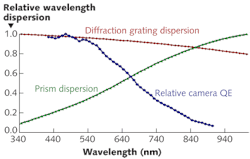
Optimizing the size and weight of any spectrometers can be a juggling act depending on the application. When imaging spectrometers are used with a telescope or microscope to image an FOV onto the entrance slit, it can be a challenge to get enough light through the system with a slit width much less than 25 µm. This challenge, as well as the size of the CCD chip and any linear dispersion in the system, combines to define the focal length and groove density of the grating if this is to be the wavelength-dispersive element. The same is true for a prism system except that only the focal length is really negotiable.
Our PARISS prism-based imaging spectrometer covers the entire spectral range from 365–920 nm, is about 200 mm in length, and weighs approximately 2 kg—much of which is due to the scientific CCD camera. A comparable grating system is likely to be about the same size and weigh up to 3 kg. The high optical efficiency, imaging integrity, and immunity from diffraction effects makes prism-based imaging spectrometers a compelling addition to the spectroscopist's tool box.
REFERENCES
- D.T. Dicker et al., Cancer Biology and Therapy 8, 1033–1038 (2006).
- J. Aaron et al., Nano Letters 9, 10, 3612–3618 (2009).
- M.P. Chrisp, "Aberration-Corrected Holographic gratings and their mountings," in Applied Optics and Optical Engineering, R.R. Shannon and W.C. Wyant, Editors, Academic Press, London, 391–451 (1987).
- E. Loewen and E. Popov, Diffraction Gratings and Applications, Marcel Dekker, New York, NY (1997).
- J. Reader, J. Opt. Soc. Am. 59, 1189–1196 (1969).
- X. Prieto-Blanco et al., Opt. Exp. 14, 20, 9156–9168 (2006).
- J.M. Lerner, Cytometry 69A, 8, 712–734 (2006).
- J. James and R. Sternberg, The Design of Optical Spectrometers, Chapman & Hall, London (1969).
- D. Warren et al., "Compact prism spectrographs based on aplanatic principles," Opt. Eng. 36, 1174–1182 (1997).
Jeremy Lerner is president of LightForm Inc., 825C Merrimon Ave., Suite 351, Asheville, NC 28804; e-mail: [email protected]; www.lightforminc.com.