INTEGRATED OPTICS: PLCs move into advanced optical instrumentation
ASHOK BALAKRISHNAN and MATT PEARSON
Optical instruments generally include light sources, various optical elements to process light signals, and photodetectors. Traditionally, these instruments were made using bulk optics, and as a result, miniaturization and ruggedization were extremely challenging. Now, planar lightwave circuits (PLCs) can integrate a number of optical elements onto a single optical circuit, resulting in improved size, cost, and functionality. As a result, these optical chips are being used increasingly for optical instrumentation applications.
One of the earliest uses of PLCs was for multiplexing and demultiplexing signals in telecommunications networks, where several signals are carried on different wavelengths. Arrayed-waveguide-grating (AWG) devices slowly replaced bulk-grating and filter devices as AWG performance specifications improved. Optical splitters shared many of the same size and cost advantages. However, from the 1980s to the early 2000s, this was primarily the extent to which PLCs replaced bulk optics. In fact, it was long assumed that multichannel applications were the only ones that could take full advantage of the size reductions provided by PLCs.
Technology boost from FTTH
In the early 2000s some applications arose, in spectroscopy and in fiber-to-the-home (FTTH), that started to challenge this assumption. For instance, FTTH chips that operated on only two channels had a revolutionary effect on how photonic chips were used in optical systems. In this case, the channels were each very broad, with a 20 to 100 nm width, and operated bidirectionally in the same waveguide and optical fiber. Densely packed PLC chips were designed to handle these requirements, incorporating wavelength-division multiplexing, lasers, detectors, and other optical elements on a single chip. Despite the apparent simplicity of this application, PLCs still provided substantial cost and size reductions over their bulk counterparts, with hundreds or even thousands of devices fabricated on each silicon wafer.
It is relatively easy to incorporate wavelength splitting and basic power splitting into PLCs. However, many more functions are required for a sophisticated optical instrumentation application. Over time, waveguide designers have developed many significant optical elements on PLCs, including N × M splitters that are virtually insensitive to wafer fabrication nonuniformities, ultralow-backreflection fiber-to-waveguide couplers, and other passive structures.
Alignment of active components
Active functions are also crucial to every optical instrument. The hybridization of lasers began in the early days of FTTH and has been perfected to achieve very good optical coupling even in high-volume processes. Lasers can now be passively coupled to PLC waveguides with coupling losses approaching 0.5 dB, entirely through computer vision and robotic die-attach. No lenses and no active alignment are needed. Complex but highly reproducible photolithography and etching are already part of the PLC wafer process and are used to achieve high alignment accuracies for hybrid components.
In a PLC circuit, light is guided in a horizontal plane, confined by glass. Coupling this light to a detector has always been challenging. One makeshift approach to this problem is to butt-couple photodetectors to the edge of the PLC chip, where the light exits. Although this approach works, it requires active alignment, causes problems in packaging, and leads to complications in the wirebonding needed to extract the photocurrent. Robust mirror structures etched into the PLC circuit itself have been devised and fabricated that can redirect the guided light into the vertical direction. Standard surface-illuminated photodetectors can then be integrated onto the PLC over the mirrors. The top of the photodetector includes electrical pads to accommodate standard wirebonding. Avalanche photodetectors and p-i-n photodetectors can be hybridized to PLC chips this way, making a very flexible platform with yields close to 100% and collection efficiencies exceeding 96%, assembled entirely through computer vision and robotic die-attach.
Other application-specific functions, such as polarization beamsplitters and optical isolators, are also being implemented into PLCs. While the former can be done through careful process control, both can take advantage of the implementation of optical-bench techniques onto PLC. Thus, the majority of functions necessary to construct any typical optical test instrument, in a very small form factor, are available from PLCs.
It is now relatively easy to incorporate any single function, or group of functions, into a small PLC chip. Form and function can be addressed simply; however, the concept of fit poses unique challenges when multiple functions are required on the same PLC. This is the case when all or much of an optical instrument is to be reproduced on a single optical chip. Each function imposes its own design constraints and processing requirements, and all of these issues must be simultaneously addressed in order for the full system-on-a-chip to work.
Satisfying many requirements at once
Process-independent splitters, for instance, achieve their independence by requiring precise waveguide geometries, stress-canceling sacrificial features, and precise clearance from adjacent structures. Wavelength splitters require precise etch-depth control, regardless of the etch requirements of other elements. Hybridization of active elements requires metallization, which in turn imposes a temperature budget, metal-to-silica wall clearances, alignment marks, and metal deposition-thickness control.
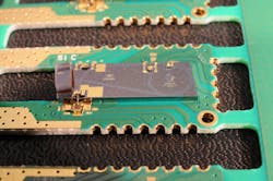
An example PLC chip that meets this high level of complexity is intended to be part of an uncompressed video link for use in a number of specific military applications (see Fig. 1). One wavelength of light is created by an onboard distributed-feedback (DFB) laser, which modulates at up to 2.5 Gbit/s to provide data and instructions to a remote module. There are two incoming light streams at two unique wavelengths, each also operating at up to 2.5 Gbit/s. Each incoming data stream provides data from different cameras. Detectors on the PLC demodulate the data into electronic pulses. A transimpedance amplifier is placed close to the photodetector to reduce wire-bond impedance. The chip also contains a front-facet monitor photodetector to eliminate laser-power drift with temperature. A lattice structure is embedded throughout the optical layer that defines areas where light is permitted to propagate within the chip. To create these optical structures in conjunction with laser and detector hybridization requires a tight link between optical layout, modeling, fabrication, and assembly.
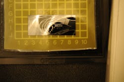
In another example, a PLC chip with a more classical waveguide design and intended for use in biophotonic applications contains, at a very high level, four interferometers configured for polarization-diverse detection (see Fig. 2). On the PLC itself, there are in fact 26 inputs/outputs, some of which are used bidirectionally. This chip contains a low-percentage power tap, nearly 20 N × M power splitters, a polarization-rotating element, and several test lines to monitor fabrication accuracy.Despite the complexity, the chip is smaller than 9 × 20 mm. The bends on each waveguide are carefully computed to reduce bend loss and polarization effects, while allowing optimum approach from one subfunction on the chip to the next. The waveguides are configured to ensure that waveguide crossings always happen at a reasonably large crossing angle. Compact routing is needed both to reduce the overall product size and to improve the on-chip uniformity. Minimum waveguide gaps are respected at all times to virtually eliminate crosstalk (to nearly a -70 dB level depending on the guide). Because of the complexity, an automated computer-optimization routine is needed to create the design and translate this design into a photolithography mask set.
PLCs can also be used in other biophotonic applications. Biochemical reactions are often monitored with fluorescent tags keyed to specific chemicals. The presence of an analyte is indicated by the strength of fluorescence at a specific wavelength. Silica is transmissive from the infrared to slightly into the UV (0.3 to 2.0 μm). A PLC chip can provide the fiber-coupled laser excitation source, and it can spectrographically isolate and detect fluorescence. Such applications have been slow to be adopted because of the large variety of applications, each of which uses different wavelength schemes. Standardization of these schemes will ease the adoption of PLC technology for biophotonics.
Ashok Balakrishnan is director of product development and Matt Pearson is vice president, technology at Enablence Technologies Inc., Ottawa, ON, Canada; e-mail: [email protected]; www.enablence.com.

