LASER DIODES: Ge-on-Si laser will integrate with optoelectronics
Large-scale integration of electronics with photonics on silicon (Si) chips will eventually make optical communications possible not just between computers, but inside them as well–in the form of interchip and even intrachip optical links. One of the more difficult photonic elements to integrate onto Si is the light emitter (which could take the form of an LED or a laser but is preferably a laser due to its much higher brightness); the reason is that Si, even when doped, is very difficult to make into a light source.
A group of researchers at the Massachusetts Institute of Technology (MIT; Cambridge, MA) is pursuing an alternate approach by creating light emitters from germanium (Ge) grown on Si.1 Unlike III-V semiconductor-laser materials (such as indium gallium arsenide or indium gallium arsenide phosphide), Ge can be easily deposited onto Si. In addition, the Si semiconductor industry is already used to working with Ge (for example, as a dopant), making the potential move to production of Ge-on-Si easier.
The big problem with Ge is that, like Si, it is an indirect-bandgap semiconductor, meaning that it normally can't be pumped to produce light. But by putting the Ge under tensile strain and adding the right amount of n-type doping, the MIT researchers got an experimental Ge-on-Si device to not just emit light but to lase as well.
Creating tensile strain
To create the device, the researchers grew a multimode Ge waveguide on Si by ultrahigh-vacuum chemical-vapor deposition at a temperature of 650°C such that the Ge was under no strain. When the Ge-on-Si cooled to room temperature, however, the two materials contracted at different rates, resulting in a 0.24% tensile strain for the Ge. This shrank the direct bandgap of the Ge, reducing the energy difference from its indirect bandgap. During the growth, the Ge was also doped with phosphorus to an amount of 1 × 10¹⁹ atoms/cm3, further reducing the direct/indirect bandgap energy difference.
The waveguide is 1.6 × 0.5 µm in cross-section, 4.8 mm long, and mirror-polished at both ends. Light from a 1064 nm Q-switched laser pulsed at a 1 kHz repetition rate was used to pump the waveguide. The 1.5 ns pulses were focused onto the full length of the Ge waveguide, resulting in a peak pump-power density absorbed by the Ge of about 300 kW/cm2.
As the pumping level was increased, the device began to lase, producing light in several peaks clustered around 1600 nm; the widths of the strong peaks at 1594, 1599, and 1605 nm decreased at increased pumping levels. In addition, the polarization changed from mixed TE/TM to mostly TE (a 10:1 ratio), which is typical lasing behavior. The researchers believe that the multiple spectral peaks result from multiple guided modes in the waveguide.
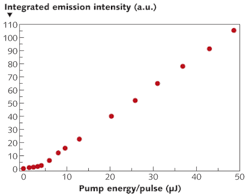
The device also shows typical laser threshold behavior (see figure). The threshold pump energy is about 5 µJ, with an absorbed pump-power density at threshold of about 30 kW/cm2. If the Ge-on-Si laser were electrically instead of optically pumped, the corresponding injection-current density would be 35 kA/cm2.
Steps to an electrically injected laser
The MIT researchers are not newcomers to this field. For instance, last year they demonstrated direct-gap photoluminescence in Ge-on-Si, electroluminescence in n-doped tensile-strained Ge-on-Si LEDs, and optical gain (although not lasing) at room temperature.2, 3, 4 The fact that they had earlier demonstrated an electrically powered Ge-on-Si LED, combined with their fabrication of a room-temperature optically pumped laser from the same material combination, means that the creation of an electrically pumped Ge-on-Si laser is within reach. Once this is achieved, it's just a matter of improving the efficiency of the laser, creating complete photonic/electronic interconnects, and getting the semiconductor industry started on a path similar to the one that began the electronics revolution.
REFERENCES
- http://www.opticsinfobase.org/ol/upcoming_pdf.cfm?id=121712
- X.C. Sun et al., Appl. Phys. Lett. 95, 011911 (2009).
- X.C. Sun et al., Opt. Lett. 34, 1198 (2009).
- J.F. Liu et al., Opt. Lett. 34, 1738 (2009).
About the Author

John Wallace
Senior Technical Editor (1998-2022)
John Wallace was with Laser Focus World for nearly 25 years, retiring in late June 2022. He obtained a bachelor's degree in mechanical engineering and physics at Rutgers University and a master's in optical engineering at the University of Rochester. Before becoming an editor, John worked as an engineer at RCA, Exxon, Eastman Kodak, and GCA Corporation.