PHOTOVOLTAICS: Photoluminescence imaging speeds solar cell inspection
THORSTEN TRUPKE and WAYNE MCMILLAN
Laser-based photoluminescence imaging is a technique for rapid characterization of silicon samples by revealing a host of material and device properties. With acquisition times of typically a few seconds or even fractions of a second, megapixel luminescence images can be captured of silicon bricks, unprocessed and partially processed wafers, and fully processed cells. The quantitative luminescence imaging applications that have been developed over the last few years open up intriguing possibilities for inline process monitoring during silicon solar cell production.
Photovoltaics (PV) technology has grown into a substantial industry with annual revenues in 2009 estimated to be more than $40 billion, and it is expected to continue growing exponentially over years to come. The majority of PV manufacturing capacity is in wafer-based crystalline silicon solar cells; in 2008 the PV industry consumed 68% of silicon feedstock and has thus become the main consumer of silicon. So-called grid parity (the point at which an alternative means of generating electricity is equal in cost, or cheaper than grid power) is within reach in many countries but requires further improvements in manufacturing efficiency and yield to achieve necessary cost reduction.
Achieving high production yield at lower cost requires advanced process monitoring tools that allow inspection with high lateral spatial resolution of specific electronic and device parameters at various parts of the PV value chain at line speed on every sample. Sample throughput in PV manufacturing is up to 3600 wafers per hour. Existing measurement techniques, which in many cases were developed for much smaller sample throughput in microelectronics applications, are unable to fulfill such requirements—they are either too slow or cannot provide sufficient spatial information or both.
Photoluminescence (PL) imaging of silicon bricks, wafers, and solar cells has been developed over recent years. Compared to measurement techniques such as microwave photoconductance decay (μ-PCD) mapping, PL imaging offers vastly superior speed and spatial resolution, making it perfectly suited for process monitoring in production. Developed by researchers at the University of New South Wales (UNSW) in Sydney, the patented technology enables PL images to be measured with acquisition times less than 1 s.1 Only a few years after its introduction, research institutes and silicon wafer and solar cell manufacturers worldwide use commercial PL imaging equipment, which is offered by BT Imaging, a UNSW spin-off company.2
How it works
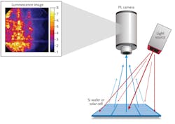
In PL imaging of silicon samples, the entire surface of the sample—typically 156 × 156 mm—is illuminated homogeneously. The external optical excitation stimulates luminescence emission from the sample, which is captured with an infrared (IR) camera. In other words, a photograph is taken of the luminescent sample (see Fig. 1). With both excitation and detection being optical signals, PL imaging is contactless and can be applied to a wide range of samples, including silicon bricks and wafers. The measured luminescence comes from spontaneous emission within the sample; hence, the PL intensity allows assessment of the bulk electronic quality inside the sample. So photoluminescence imaging can be likened to x-ray imaging of wafers and cells.
Experimental challenges in PL imaging applications are: a) the required continuous optical power of typically 100 mW/cm2 over an area of at least 156 × 156 mm; b) the need for homogeneous illumination over that area; and c) the low luminescence quantum efficiency from silicon. For example, on some of the measurements on as-cut wafers discussed further on, the number of luminescence photons emitted by the sample per incident photon is as low as 10-8.
High-power near-IR fiber-coupled laser diodes are often used as light sources in PL imaging. They provide the required high total optical continuous-wave power of more than 50 W, are sufficiently monochromatic and can easily be collimated to allow separation by optical filtering of the weak luminescence signal from the orders-of-magnitude stronger reflected excitation signal, and they can be turned into uniform illumination sources over large areas using customized beam-shaping optics. Furthermore, they are cost-effective, which is particularly relevant for inline PL imaging in PV production.
Applications
The production of a standard industrial solar cell includes the casting of feedstock into silicon ingots, cutting of ingots into bricks and wafers, and finally the processing of wafers into solar cells. The key quality parameter of the finished solar cell is its solar energy conversion efficiency. The latter depends strongly on the electronic material quality, which is given by the so-called excess minority carrier lifetime, and by device parameters such as the series resistance. Special PL imaging applications to assess these parameters have been developed with applicability across the entire PV value chain. Often these applications involve measuring and analyzing two or more images taken under different excitation and/or detection conditions.
Bulk lifetime measurements on silicon bricks: Application of PL imaging to silicon bricks prior to wafer cutting allows assessment of the electronic material quality at an early production stage. A PL image taken on the side facet of a 24 × 15.6 cm silicon brick can be calibrated into a color scale that represents the bulk minority carrier lifetime in microseconds (see Fig. 2).3 Measurement time for this image was 30 s. The same measurement with equivalent spatial resolution using conventional μ-PCD mapping would take several hours. A further advantage of PL imaging is that it allows measurement of the so-called "bulk minority carrier lifetime," a more relevant physical quantity in practice than the "effective minority carrier lifetime," which is measured by μ-PCD mapping. The bulk lifetime information from PL can predict wafer quality and provide feedback on feedstock quality as well as offering a fast process monitoring tool that allows process optimization and process excursions to be detected early. An example of process excursions in production is the formation of slip lines in monocrystalline silicon ingots, which can be reliably detected by PL imaging on silicon ingots and slabs without the need for any surface preparation.4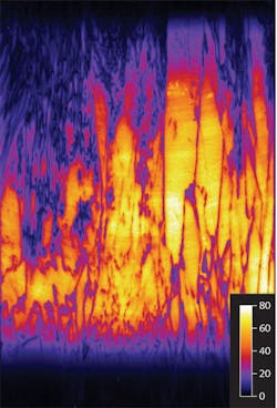
Photoluminescence imaging of silicon bricks, wafers, and solar cells has seen rapid development since its introduction in 2005. The application of PL imaging is not limited to the specific applications mentioned here. A large number of additional applications have now been demonstrated and that number is growing even more rapidly with the availability and penetration of commercial PL imaging systems offered by BT Imaging. The company recently launched specialized equipment for inline quality control and process monitoring. With its combination of speed and high spatial resolution, PL imaging is on the verge of being adopted for inline monitoring in PV manufacturing. It can also be expected to find applications in other arenas, such as the semiconductor and LED industries.
REFERENCES
1. T. Trupke et al., "Photoluminescence imaging of silicon wafers," Appl. Phys. Lett., 89, p. 044107 (2006).
2. www.btimaging.com
3. T. Trupke et al., "Photoluminescence imaging on silicon bricks," 24th European Photovoltaic Solar Energy Conf., Hamburg, Germany (September 2009).
4. W. McMillan et al., "Slip line detection on mono ingots and wafers at production throughput using photoluminescence," 25th EPVSC, Valencia, Spain (September 2010).
5. M. Demant et al., "Analysis of luminescence images applying pattern recognition techniques," 25th EPVSC, Valencia, Spain (September 2010).
6. J. Haunschild et al., "Comparing luminescence imaging with illuminated lock-in thermography and carrier density imaging for inline inspection of silicon solar cells," 24th European Photovoltaic Solar Energy Conf., Hamburg, Germany (September 2009).
7. W. McMillan et al., "In-line monitoring of electrical wafer quality using photoluminescence imaging," 25th EPVSC, Valencia, Spain (September 2010).
8. T. Trupke et al., "Spatially resolved series resistance of silicon solar cells obtained from luminescence imaging," Appl. Phys. Lett., 90, p. 093506 (2007).
9. A.S.H.v.d. Heide et al., "Mapping of Contact Resistance and Locating Shunts on Solar Cells Using Resistance Analysis by Mapping of Potential (Ramp) Techniques," 16th EPVSC, Glasgow, UK (2000).
Editor's note: Find out more about the market for photovoltaic equipment and market outlook at the 2011 Lasers & Photonics Marketplace Seminar in January. For information or to register, visit www.marketplaceseminar.com.
Thorsten Trupke is a founder and CTO, and Wayne McMillan is VP, sales & marketing, at BT Imaging Pty Ltd., 2-12 Foveaux Street, Surry Hills, NSW, 2010, Australia; e-mail: [email protected]; www.btimaging.com.