NANOMETROLOGY: Nanoscale measurement tests metrologists
VLADIMIR UKRAINTSEV and BILL BANKE
Physical properties of nanometer-sized objects and the consequent quality of nanometer-sized products depend strongly on their dimensions. Control of critical dimensions (CD) is vital for overall success when working at the nanoscale. Metrology is a key component of both process and quality control. But what is nanometrology, and does it differ from metrology at the macro-, mini-, and micro-scale?
Modern nanometrology is based largely on knowledge accumulated over the last 10–20 years of semiconductor technology development. Critical dimension metrology in semiconductor processing entered the nanotechnology era in the late 1990s, when work on 130 and 90 nm node technologies led to the conclusion that precision is an insufficient metric for metrology quality assessment.
Measurement uncertainty as a quality metric
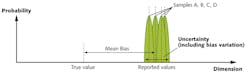
Through research and daily practice in the semiconductor industry it became obvious that other components of measurement uncertainty (MU) must be considered.1,2 Two components became particularly noticeable, namely sample-to-sample measurement bias variation and sampling uncertainty.3,4 The first of these (sample-dependent systematic error) is significant for commonly used CD metrologies such as top-down and cross-sectional scanning electron microscopy (SEM) and optical scatterometry (OCD). Unless special measures are taken, bias variation of critical dimension SEM and OCD could exceed several nanometers (see Fig. 1).5,6,7 The measurement uncertainty of the CD SEM also grows with various degrees of measurand complexity (see Fig. 2). The measurand is the property of the object to be measured. In this example, the total measurement uncertainty (TMU) of the CD SEM is shown as a function of the feature-shape variation caused by the changes of lithography scanner focus—TMU is an IBM-defined metric in units of nanometers that captures additional (beyond precision) components of uncertainty of the measurement system under test, in this case the CD SEM.8 A reference metrology (RM) system is required to evaluate the TMU of a system under test. Here a CD atomic force microscope (AFM) was used as the trusted reference system.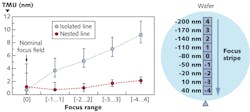
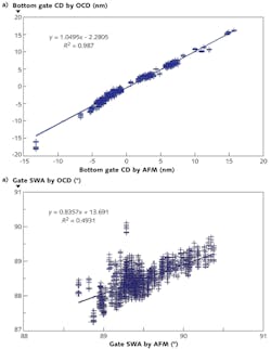
As a general rule of thumb, the measurement uncertainty should only consume a maximum of 20% of the process tolerance budget. The data from Fig. 3 also show the OCD fleet TMU for sidewall angle measurements is estimated as ±0.8°. This level of uncertainty is not acceptable because SWA process tolerance for that technology was ±1.6°. This leads to TMU/T ratio of 0.5, which exceeds the required limit of 0.2 for the ratio. The OCD single tool precision is ±0.2°.
If this single tool precision (P) was used to evaluate quality of the SWA metrology, a result of P/T = 0.2/1.6 = 0.12 would significantly overestimate the SWA measurement capability of the OCD. There is a danger here. Clearly, this shows the importance of using an uncertainty estimate (TMU) instead of just a precision estimate for estimating a measurement technology's ability to control a process.
Role and choice of reference metrology
Variation of measurement bias and, therefore, MU can be assessed only if a reference metrology is used. What is reference metrology? An ideal RM system provides SI-traceable measurements with known (and sufficiently low) uncertainty. A nanometer-level MU of CD metrology tools is needed to control manufacturing of products with CDs below 100 nm. The required MU of modern semiconductor RM systems is in the sub-nanometer range. The choice of RM tools with such high quality is very limited. To search for the best RM technique, one could try to estimate MU of various CD metrology techniques.9
Table 1 shows measurement uncertainty estimates for five of the most common metrology techniques for one specific application. The most significant components of measurement uncertainty such as an accuracy of scale calibration, repeatability, sample-to-sample bias variation, and sampling uncertainty were added together. The combined uncertainty for a single site measurement (column 6) and uncertainty of the mean for typical sample size (column 8) are shown.
In brief, low sample-to-sample bias variation (intrinsic relative accuracy) and high sampling efficiency make CD AFM a good candidate for linewidth reference metrology. Sampling efficiency refers to the amount of sample averaging built in to a single measurement. For example, a measurement requiring the cross-sectioning of the sample specimen has a low sampling efficiency because considerable effort goes into the sample preparation and it yields a limited amount of sampling.
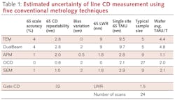
Transmission electron microscopy (TEM) has presumably the lowest sample-to-sample bias variation of all the considered techniques. Scale accuracy of TEM can be also significantly improved if a crystalline sample with known lattice parameters is used. However, sampling uncertainty of TEM measurements is very high due to low sampling efficiency. This is related to local linewidth variation of the sample and can be suppressed to a nanometer level, but only with an extraordinary effort (by averaging tens of TEM measurements, each done using independent samples representing the same measurand). Therefore, TEM can be used as an RM tool but the approach is extremely costly and time consuming.
Widely used in nanotechnology, top-down and cross-sectional SEM and OCD tools do not meet strict MU requirements of nanometrology unless they are properly calibrated and their bias is corrected. The bias correction procedure may be very convoluted, so these measurement technologies need supporting metrology such as RM.10
Future
Various techniques could be considered as a reference metrology system. Each would have strengths and weaknesses. Some time ago the idea of hybrid metrology surfaced, the goal being to improve the accuracy of a high-throughput inline or reference metrology tool by combining its measurement with that of another measurement.11 It doesn't have to be, but the complementary metrology could be another measurement technology. Hybrid metrology uses the strengths of two or more measurement techniques with a goal of minimizing the uncertainty of a particular measurement.
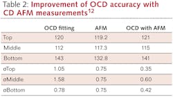
In a recent example of this approach, the OCD measurement was supplemented with that of a CD AFM and significantly improved the OCD measurement uncertainty, while still able to maintain its high throughput.12 Table 2 shows the benefit of using the CD AFM in concert with the OCD measurement. The table shows the top, middle, and bottom linewidth measurement averages and MU values from the OCD both with and without the supplemental CD AFM measurements. It is noteworthy that the top linewidth OCD average shown in the first row assisted by the CD AFM did not position itself between the separate OCD and CDAFM averages. It is also important to note that the uncertainties of all OCD measurements were significantly improved with the aid of the CD AFM and surpassed the uncertainties of the CD AFM itself! This is a convincing example of the benefit of combining metrology in new forms of hybrid techniques. Significant improvements in reference metrology and inline CD metrology are still needed to support nanotechnology research, development, and manufacturing. The future of nanometrology will benefit from the synergy of various measurement technologies and methodologies.
REFERENCES
1. W. Banke and C. Archie, "Characteristics of CD accuracy," Proc. SPIE, 3677, 291-308 (1999).
2. International Technology Roadmap for Semiconductors, 2007 edition (http://www.itrs.net).
3. V. Ukraintsev, "Effect of bias variation on total uncertainty in CD measurements," Proc. SPIE, 5038, 644-650 (2003).
4. B. Bunday et al., "Impact of sampling on uncertainty: semiconductor dimensional metrology applications," Proc. SPIE, 6922, 69220X (2008).
5. V.A. Ukraintsev, M.C. Tsai, T. Lii, and R.A. Jackson, "Transition from precise to accurate critical dimension metrology," Proc. SPIE, 6518, 65181H (2007).
6. N. Rana et al., "The measurement uncertainty challenge of advanced patterning development," Proc. SPIE, 7272-2 (2009).
7. V.A. Ukraintsev and J. Foucher, "Dimensional metrology with sub-nanometer uncertainty: unique role of AFM as the reference," Proc. SPIE, 7638, 76381C-76381C-8 (2010).
8. M. Sendelbach, M. and C. Archie, "Scatterometry precision and accuracy below 70nm," Proc. SPIE, 5038, 224-238 (2003).
9. V.A. Ukraintsev et al., "The role of AFM in semiconductor technology development: the 65 nm technology node and beyond," Proc. SPIE, 5752, 127-139 (2005).
10. V. Ukraintsev, "Role of CDAFM in achieving accurate OPC modeling," Proc. SPIE, 7272, 727205-727205-8 (2009).
11. S. Muckenhirn, "Integrated measuring instrument," Patent US 6,986,280 B2 (pub. date: Sept. 11, 2003).
12. R. Silver et al., "Improving Optical Measurement Accuracy using Multi-Technique Nested Uncertainties," Proc. SPIE, 7272, 727202 (2009).
13. V. Ukraintsev and W. Banke, "Reference metrology for nanotechnology: significance, challenges and solutions," Proc. SPIE, 7762, 776212 (2010).
Vladimir Ukraintsev is president of Nanometrology International, Inc., and Bill Banke is a self-employed metrology contractor, in Allen, TX; e-mail: [email protected]; www.nanometrology.net.