OPTICAL SURFACE PROFILING: Profilometer advances benefit surface analysis, film-thickness measurement
KLAUS FREISCHLAD
An optical profiler produces a detailed three-dimensional (3-D) surface map of a test area with Angstrom-level height resolution that can be further analyzed according to the specific requirements of each application. An analytical technique that is essential in many industries, optical profilometry is used to characterize, for example, residual roughness of super-polished optical surfaces, the material hardness and wear of metal bearing surfaces, the dissolution kinetics of minerals, the texture properties of disc media, and the surface shape of microlenses, among many other applications.
In addition to surface topography, the film thickness of transparent layers on sample surfaces can be measured simultaneously at high resolution. Such thickness measurements include, for instance, the layer thickness of anticoagulants on heart stents and the films and scribe line properties of solar cells. While the basic principles of optical profilers have been in use for more than 20 years, recent technical advances related to system components and improved data processing are enabling enhanced system performance and usability.
Interference microscopes
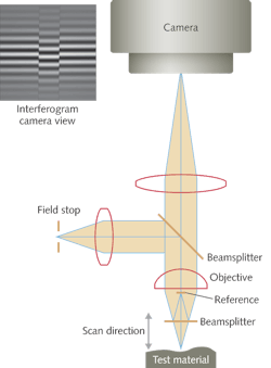
One class of optical profilers is interference microscopes with computerized data acquisition and analysis. Here the relative position of the test surface with respect to the optical system is scanned vertically during measurement. Just as in a standard epi-microscope, the test surface is illuminated through the microscope objective and is imaged onto a CCD-camera, which saves the images in the system computer. In most cases, the actual interferometer is placed between the microscope objective and the test surface (see Fig. 1). For the Mirau-type interference objective shown, the illuminating beam is partially reflected by the lower beamsplitter surface and partially transmitted to the test surface. After these two beams are reflected by the reference and test surface respectively, they recombine at the beamsplitter and travel to the camera.
The camera image (top left) shows the test surface overlaid with bright and dark interference fringes that can be interpreted as contour lines of the surface with a height spacing of half the wavelength of the light used, typically around 280 nm for visible white-light illumination. Note that the fringes don't cover the whole image but only a limited surface height range. This is due to the use of broadband white light with a limited coherence length within which fringes can appear. This use of broadband light and vertical scanning over the full height range of the test surface is called white-light scanning interferometry. Alternatively, the use of a coherent monochromatic source with fringes covering the whole field of view, together with only a short vertical motion for fringe modulation, is called phase-shifting interferometry. While the former is suited for test surfaces exhibiting a large height range, the latter requires that the whole test surface is in good focus during data acquisition.
To obtain the 3-D topography map of the test surface, the test piece (or optical system focus) is scanned vertically while a sequence of camera images is acquired. Sophisticated signal processing algorithms are applied to the fringe signal at each camera pixel and provide robust low-noise height data with a height resolution down to 0.1 nm RMS and below. The total information in a 3-D surface map is given by the number of independent 3-D resolution elements in the map—a number that depends on the lateral and vertical resolution as well as the field size and vertical extent of the map. The lateral resolution is fundamentally limited by optical diffraction, whereas the vertical resolution is given by the vertical measurement noise. A good profiler system will match the optical resolution with the pixel sampling of the camera while maximizing the size of the field of view. Scientific-grade high-resolution imagers with 2048 × 2048 pixels—used in state-of-the-art optical profilers—provide large field coverage as well as the high pixel count necessary to adequately sample the images.
Advances promote ease of use
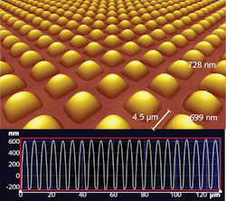
Compared to less sophisticated profilers with cameras of typically 640 × 480 pixels, new large-field imaging and high pixel sampling combine to increase the resulting information content by an order of magnitude. This is important for a variety of applications, including the statistical characterization of rough surfaces, the location and review of defects, the inspection of microlenses, and the investigation of corrosion effects of bacteria on mineral surfaces (see Fig. 2, top). In another application a large number of microlenses on the pixels of a CMOS imager can be quickly inspected in a single map (see Fig. 2, bottom).
The large amounts of data that result from the high-resolution imagers, and, even more so, from the large stitched maps, place a large burden on the processing computer. The latest multicore processors and optimized software with 64-bit addressing and multithreading can easily handle these demands and provide fast data analyses with responsive display of the measurement results. Without these latest developments, operator interaction would be unusable.
Besides sophisticated processing algorithms, optical profilers require good lateral resolution of the surface maps, as well as good height fidelity of small surface features. This necessitates that during data acquisition the test surface is in best image focus exactly when the highest contrast fringes are present—that is, the fixed reference surface of the interference objective must be adjusted to be in best focus. For high magnification objectives with corresponding high NA, the depth of focus is very small (a 100× objective with an NA of 0.7 has a depth-of-focus of ±0.56 µm). On this scale, the temperature environment of the profiler seriously affects the reference focus, and even only one degree of temperature change affects measurement precision and repeatability. While athermal designs for 50× objectives have become state-of-the-art, the latest development of an athermal 100× Mirau objective represents an important improvement in profiler usability at highest resolutions.
Klaus Freischlad is director of optical systems engineering at Zemetrics Inc. 3708 E Columbia St. Ste.110, Tucson AZ 85714-3413; e-mail: [email protected]; www.zemetrics.com.