PHOTONICS APPLIED: PHOTOVOLTAICS: A sunny outlook for lasers in solar

The mere whisper of “solar” within the corridors of tool suppliers has long been associated with feelings of excitement, claims of altruism, and images of dollar signs. And the laser industry is by no means immune to such uncontrollable giddiness. As a prospective candidate for the “next-big-thing,” it doesn’t get more tantalizing than solar. Recently, however, in the wake of macroeconomic meltdown, unbridled excitement has been replaced by guarded optimism that solar can sustain its growth appeal amid otherwise bleak forecasts for industrial lasers.
With solar/photovoltaics being a new and emerging segment for lasers, uncertainty permeates in equal measure across the two sectors: for solar, how to realize the potential return-on-investment (ROI) of lasers; and for the laser industry, what fuels the demand for laser tooling within photovoltaics? Combining recent solar analysts’ projections of supply and demand with the latest technical innovations (next-generation cells and new industrial-grade lasers) helps paint the landscape for lasers in solar over the next decade.
Laser entry in the solar industry
The pull of solar on lasers started with groundbreaking research performed during the 1980s and 1990s at the University of New South Wales (UNSW; Australia) using crystalline silicon (c-Si) cells, and—for thin-film types—at various labs within North America.1, 2 The research analyzed a plethora of laser-based processes applicable to each competing cell architecture; the underlying motivation for lasers was to identify methods of material-removal during cell and panel production. In the majority of c-Si and thin-film types, the absorber materials and neighboring thin-film layers possess absorption characteristics overlapping with laser wavelengths from the deep-UV to the near-infrared (IR).
This relationship naturally prompted evaluation of pulsed solid-state lasers operating at fundamental wavelengths (approximately 1 µm) or harmonics (532, 355, and 266 nm). Sadly, the timing was out of sync. First, because the absence of industrial-grade, diode-pumped solid-state (DPSS) lasers at the time, but also because the solar industry was still ten years away from bursting to life or becoming a priority to equipment suppliers. A precedent was set though. By sampling the virtues of solid-state lasers from infancy, the solar industry rapidly established a hierarchy of laser types, with DPSS lasers in the pole position.
This initial flurry of research highlighted several fundamental issues that are still relevant today. First, production of c-Si cells is readily achieved using conventional (nonlaser) equipment. The majority of c-Si lines installed before 2005 used multiwire slurry saws (MWSS), deposition equipment (especially PECVD), etching tools (both plasma and chemical), diffusion furnaces, and screen-printers—no standard laser-based tools required. Second, lasers find their raison-d’être within next-generation high-efficiency c-Si concepts, but still only if they provide significant ROI. And third, all thin-film production lines utilize lasers as essential tools for the panel-to-cell interconnection and isolation stages (known as P1, P2, and P3 patterning).
So when pilot thin-film lines were first configured, DPSS lasers had been designed-in as standard tools. Further, thin-film patterning has high laser unit consumption. Each line has three distinct patterning stages; large-panel-size fabs (Gen. 5 or higher) can require multiple lasers per patterning step. This ensured that thin-film production rapidly became the dominant segment for laser revenues within solar, a position retained today (see Fig. 1). Interestingly, this segmentation is at odds with end-user deployment, in which c-Si cells account for more than 90% of panels installed.
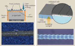
In c-Si production, laser tools have emerged as an alternative approach for a process known as edge (or junction) isolation.3 This step ensures that front and back contacts are electrically isolated when finished cells exit production. Competing technologies include plasma etching (removes material from the edges) and chemical etching (removes the rear n-type layer). Plasma was the front-runner due to low capital cost and ease of use; chemical etching is favored by turnkey line suppliers who utilize chemical etching for other processes (saw damage removal, front-side texturing, phosphorous silicate glass removal). Therefore, laser-tools had to prove their worth vs. an incumbent technology, compounded by lasers being somewhat out of the comfort zone of c-Si producers and line suppliers.
Pre-empting solar industry focus on c-Si efficiency enhancement, one laser-based process was introduced by an early market leader, BP Solar. Its “Saturn” lines used a technique discovered at UNSW: laser grooved buried contacts (LGBC).4 This multistage process uses lasers to scribe trenches during front contact formation, which permits additional (selective) doping, recessed emitters for reduced finger line-width shading, high-conductivity electroless plating, and high metallization aspect ratios—all efficiency-enhancement steps. But again, the timing was off. Industrial lasers did not meet throughput requirements, nor were dedicated tools available for automated wafer handling. Despite low uptake from the industry, the legacy of the LGBC concept (and laser-based efficiency enhancement) is seen today in current proposals for high-efficiency cells: selective emitters, dielectric ablation, and dopant diffusion. Though LGBC provided a glimmer of hope for lasers, solar again had to wait years for suitable lasers.
The roadmaps converge
Laser adoption within the solar industry has now reached an inflection point. From a market-pull perspective, this is created by turbulence within the capacity expansion plans of cell and panel producers. First, the supply-demand relationship for solar production has evolved due to a complex mix of variables: government incentives coming online rather unpredictably (Spain, Italy, Greece, France, and USA, for instance); uncertain credit availability for capacity expansions; delays in utilization ramp-up of thin-film production-line suppliers; and the rate at which the all-important dollar-per-watt metric at the balance-of-system level has declined. While the solar industry has basked in annual growth rates above 40%, volatility with cyclic behavior is certain to occur in the short-term (see Fig. 2). Solar equipment revenues for 2009 are forecast to grow at “only” 10%, albeit subject to a few wildcards.5End-user demand aside, supply is not a problem. Indeed, alarm bells have been sounding “oversupply” and “inventories” for some time; such is the wealth of new producers that have flocked to solar recently. Consequently, favored analyst buzzwords today are “consolidation,” “fall-out,” and “merger-and-acquisition.” But such a pause in solar’s relentless capacity drive is not a bad thing for an emerging technology such as lasers. To succeed within a market in which supply exceeds demand, technology differentiation becomes a top priority. And this need ultimately provides demand for new equipment to accelerate both the introduction of high-efficiency cell concepts and decreased manufacturing costs specific to large plants (GW-fabs). Now lasers have garnered renewed interest from the solar industry—as a necessity, not a luxury.
Within thin-film production, lasers will retain preferred-equipment status for patterning. This status, however, comes at a price, or more specifically, the impact on average selling price (ASP). As an established process, the ASP of laser patterning tools will undergo price erosion throughout the supply chain. Further, the request now is for more-compact lasers with faster throughput (repetition rates) and better reliability than the solar industry has experienced so far.6 New applications for lasers in thin-film markets will only emerge if lasers show tangible ROI compared to existing technologies. Options include border deletion (competitive with sandblasting) and solar glass cutting (competitive with mechanical cutters).
The prospects for increased laser adoption within c-Si production are more appealing than for thin-film. Several factors drive this sea change. With a greater number of established c-Si producers, there is fierce competition to improve efficiency and reduce manufacturing costs; with a few exceptions (like back-junction and “HIT” cells), the majority of c-Si modules are composed of moderate-efficiency cells (14% to 16%) manufactured using “low-risk” heritage tooling; as silicon material is the major contributor to cost throughout the value chain, continued silicon reduction will move the average wafer thickness below about 180 mm. This promotes noncontact-based tooling to avoid yields dropping unacceptably.
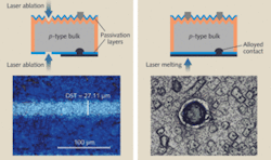
Many applications are proposed for lasers in next-generation c-Si production lines.7, 8 However, a common theme behind many of these applications relates to the contact-formation stages and efficiency enhancement.9 Front-surface techniques include selective removal of passivation layers (dielectric ablation), creating localized enhanced dopant regions around the emitters (dopant diffusion or selective emitters), drilling vias through the wafers to open up conducting pathways for back-contact designs (metal or emitter wrap-through), and rear-side laser firing (laser fired contacts; see Fig. 3). Excitement abounds with c-Si cell producers now when each of these is mentioned. Worthy testimony indeed to the trailblazing LGBC R&D discussed earlier.Laser adoption in c-Si also stands to benefit from recent advances in industrial lasers. But laser processing on c-Si cells is by no means easy. And the devil is in the details. Many a laser process engineer has been disappointed when seemingly immaculate laser-applications efforts were shown to fail within cell production lines. Failure is often characterized by changes in minority carrier recombination rates in bulk silicon caused by laser-induced damage (or microcracking). This can happen if any laser parameter falls out of the narrow process windows—pulse-width too long, power too high, absorption too deep, pulse-overlap too high. Indeed, applications such as c-Si front-surface dielectric ablation or dopant diffusion come to life only because short-pulse (picosecond) and short-wavelength (355 nm) industrial-grade lasers are now available. At last we see convergence of solar and laser roadmaps, if somewhat more by fortune, than by concerted synergy between the industries.
Outlook
With the general prognosis that the solar segment is to a greater extent shielded from macroeconomic depression, and plenty of opportunities for lasers to influence next-generation production tooling, engagement between the two industries should now blossom. The laser industry will welcome the implementation of new high-efficiency cell concepts. The industry will be relieved to apply industrial-grade lasers to enable this and will be happy to swap outdated technology when convinced of the laser’s beneficial ROI.
REFERENCES
- M.A. Green, Silicon Solar Cells: Advanced Principles and Practice, Photovoltaics Special Research Centre, Sydney (1995).
- A.D. Compaan et al., Optics and Lasers in Engineering 34(15) (2000); J. Bohland et al., NREL Report SR-520-35177 (2004); and references therein.
- F. Colville, Global Solar Technology, in print (2009).
- N. Mason et al., 19th European PVSEC, Paris (2004).
- http://www.semiconductor.net/article/CA6638576.html.
- C. Dunsky & F. Colville, Proc. SPIE 6871 (2008).
- F. Colville et al., Photovoltaic International 1,
- F. Colville, Photovoltaic International 3, p. 105 (2009).
- F. Colville, Photovoltaics World 1, p. 44 (2009).
- F. Colville, Lasers & Photonics Marketplace Seminar (2009).
About the Author
Finlay Colville
Dr. Finlay Colville has been Head of Research at PV-Tech and Solar Media Ltd since 2015. Before this, he spent 5 years as VP and head of solar at market research firm NPD Solarbuzz, and 10 years in various sales and marketing roles at Coherent, Inc. Dr. Colville holds a BSc in Physics from the University of Glasgow and a PhD in nonlinear photonics from the University of St. Andrews.
![FIGURE 2. Lasers within the solar industry show a strong bias toward thin-film cell types, with revenues from solid-state lasers in the IR, green, and UV dominating solar applications during 2008 [10]. FIGURE 2. Lasers within the solar industry show a strong bias toward thin-film cell types, with revenues from solid-state lasers in the IR, green, and UV dominating solar applications during 2008 [10].](https://img.laserfocusworld.com/files/base/ebm/lfw/image/2016/01/th_phot_a_02.png?auto=format,compress&fit=max&q=45?w=250&width=250)

