NEAR-INFRARED IMAGING: Hybrid photodiodes promise cost-effective short-wave IR imaging
![FIGURE 1. A shadow-cast image of a monarch butterfly (top; original in inset) illuminated at 1310 nm shows fine features, such as the limbs and the antennae. The imager (upper inset) has a resolution of 256 x 256 pixels with a pixel pitch of 154 µm. Cut-off frequencies of the diodes are shown in the Bode diagram (bottom). The inset at bottom shows a snapshot taken from a movie of two woodlice (armadillidium vulgare) illuminated at a wavelength of 1310 nm) [2].](https://img.laserfocusworld.com/files/base/ebm/lfw/image/2016/01/th_hybrid_1109_01.png?auto=format,compress&fit=fill&fill=blur&q=45?w=250&width=250)
TOBIAS RAUCH, SANDRO F. TEDDE, and O. HAYDEN
The growing interest in short-wavelength infrared (SWIR) imagers is related to the increasing number of applications in this particular spectral region. Wavelengths between the silicon bandgap limit of about 1.1 and 2 µm are of commercial interest because of the low water absorption in this spectral region. Photodiodes for the SWIR are usually made from germanium (Ge) or compound semiconductor (indium gallium arsenide (InGaAs), for instance), and sophisticated quantum-well IR photodetectors for multicolor detection. Nevertheless, high-resolution SWIR imaging remains expensive because of the nonsilicon semiconductor materials used for the fabrication of pixelated detector arrays. If critical limitations such as the costs for fabrication or the supply of low-bandgap semiconductors can be solved, than SWIR imaging has significant potential for widespread application.
Organic electronics is potentially an interesting and cost-effective alternative to solid-state devices. For imaging in the visible spectrum organic electronics has already shown promising results with solution-based semiconductors. Most recently, we have shown that effortless spray-coating is the method of choice for industrial-scale organic photodiode (OPD) fabrication with high diode rectification and high quantum efficiency.1 However, for SWIR applications at wavelengths beyond 1 µm the absorption of organic low-bandgap absorber appears to be insufficient for SWIR diodes. Hybrid diodes based on an organic semiconductor matrix with embedded nanocrystalline semiconductor particles, which act as a SWIR absorber, offer the cost benefits of both organic electronics and colloidal nanocrystals. We integrated these hybrid OPDs on amorphous-silicon imager backplanes to realize a flat-panel imager for SWIR applications that has been demonstrated to produce videos (see Fig. 1).2
Colloidal quantum dots
Organic semiconductors as polymers or small molecules have significant advantages over solid-state devices, including fabrication on large active areas, a variety of geometrical degrees of freedom, low-temperature processing, and adjustable spectral sensitivity. The ease of fabrication derives from the solution processability of these semiconducting materials–they are easily soluble in common organic solvents, which enables fast and economic device realization with standard printing techniques. Polymeric SWIR detectors have recently been reported, though good diode characteristics and high efficiencies beyond the silicon bandgap (around 1100 nm) at high reverse biases were not achieved.3
Colloidal quantum dots (QDs) represent a suitable alternative for SWIR absorbers for photodetection with solution-processed diodes. Colloidal QDs have dimensions of a few nanometers surrounded by a ligand shell and are usually obtained in a single pot synthesis. The diameter of the QDs, which can be controlled on the single-nanometer scale, determines optical properties like spectral absorption and thus the spectral sensitivity due to quantum confinement effects.
Recent published results on colloidal QD devices showed poor lifetimes of only a few weeks, which can be attributed to the tradeoff between high sensitivity with short ligands and low sensitivity with long but insulating ligands.4, 5, 6 In addition, QD films as photodiodes suffer from aggregation effects causing inhomogeneous layers. Thus, only QD thin films of about 200 nm thickness are usually reported, which is critical because thicknesses in the micron range are required for high internal quantum efficiency at the SWIR regime.
Finding the right blend
We decided to start our work on hybrid diodes with colloidal lead sulfide (PbS) quantum dots. The PbS QDs are among the very few QDs in which the synthesis can be upscaled and QDs at the gram-scale are already available. Such a solid supply of new nanoscale material is critical for industrial applications. Reported composites from QDs and organic semiconductors showed some IR sensitivity. However, the efficiencies were poor as QDs were applied to blends with either hole- or electron-conducting organic semiconductors only. This result is somewhat unsurprising as QDs with a passivating ligand shell are expected to show insufficient charge transport in the composites.
In our case, a ternary composite of electron- and hole-conducting organic semiconductor blended with the colloidal QDs yielded highly sensitive SWIR photodiodes (see Fig. 2). The diodes comprise a solution-processable photoactive absorber layer sandwiched between an indium tin oxide (ITO) anode covered by a poly(3,4-ethylenedioxythiophene): poly(styrenesulfonate) (PEDOT:PSS) interlayer and a low work function cathode (Ca/Ag or Al). The doctor bladed absorber layer consists of an hole conducting regioregular poly(3-hexylthiophene) (rr-P3HT), an electron conducting [6,6]-phenyl C61 butyric acid methyl ester (PCBM) and oleic acid capped PbS QDs as SWIR sensitizer. PbS-QDs are added to the organic semiconductor layer with a volume fraction of ~50%. A homogeneous distribution of QDs in the organic bulk was demonstrated by means of TEM analysis. Unpublished results show that our ternary absorber layer can even be fabricated with spray coating with layer thicknesses of several micrometers, which allows us to optimize the internal quantum efficiency.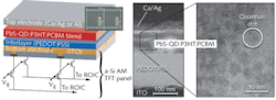
An imager with an active-matrix backplane showed both superior diode characteristics and–equally important–superior processability to reported solution-processable SWIR diodes. The devices achieved external quantum efficiencies (EQEs) of up to 51%. With glass-encapsulated hybrid diodes and operating at room temperature, the flat-panel imager is sensitive up to 1.9 µm. More detailed analysis of the imager showed low optical crosstalk between the pixels and a temporal resolution of 2.5 kHz (at -3 db) and 39.5 kHz (at -6 dB), which allowed us to record videos beyond the absorption edge of silicon at 1310 nm.2
Applications for the hybrid photodiodes are envisioned in the industrial range like process and environmental monitoring, active night vision, surveillance systems, as well as medical SWIR imaging, such as optical coherence tomography.
REFERENCES
- S. Tedde et al., Nano Letters 9, p. 980 (2009).
- T. Rauch et al., Nature Photonics 3, p. 332 (2009).
- G. Xiong et al., Science 325, p. 1665 (2009).
- G. Koleilat et al., ACS Nano 2, p. 833 (2008).
- G. Konstantatos et al., Nature 442, p. 180 (2006).
- A. S. McDonald et al., Nature Mater. 4, p. 138 (2005).
Tobias Rauch and Sandro F. Tedde are research scientists, and Oliver Hayden is program manager at Siemens AG, Corporate Technology, CT MM 1 Günther-Scharowsky Street 1, 91058 Erlangen, Germany; e-mail: [email protected]; www.siemens.com.