UV OPTICS: New optical developments boost near-UV applications
An electromagnetic-spectrum chart generally divides the ultraviolet (UV) into three areas: UV-C, typically defined as 100 to 280 nm; UV-B, (280– 320 nm); and UV-A (320–400 nm). From a more practical perspective, however, the UV spectrum can be split neatly at around 250 nm. For optics the choice of available substrate and coating materials from 100 to 250 nm (commonly defined as the deep-ultraviolet and extreme-ultraviolet, or DUV and EUV regions, respectively) is limited, their processing is expensive, and thus the applications remain relatively sparse. The application space in the near-UV region, however, is flourishing, leading to (or, perhaps, being led by) key developments in the UV optical components and coatings, as well as the UV light sources that enable them.
Materials matter
Developments in optical components really begin at the materials-science level. Much work is being done to develop materials with attractive optical properties in the UV and separate materials with attractive properties in the far-infrared. In the near-UV, choice of transmissive optical materials has historically been fairly limited.
Fused silica has been the nearly ubiquitous choice because of its high internal transmittance, low coefficient of thermal expansion, and reasonable dispersion. However, fused silica is not without its limitations, especially when it comes to fabricating precision refractive components. Its low index of refraction (less than 1.50 throughout the near-UV, visible, and near-infrared spectra) isn’t well suited for designing and fabricating optical components with a high numerical aperture. High-numerical-aperture optics, useful for collecting and refocusing very divergent light sources (such as fluorescent emission) or very weak light sources (again, fluorescent emission) are desirable in many near-UV applications.
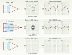
One of three possible configurations of a simple high-numerical-aperture near-UV “component” is a simple plano-convex lens fabricated from fused silica (see Fig. 1). The very steep curvature of the convex surface is immediately apparent. Not only will this surface be very difficult to fabricate, but the extreme curvature yields a focused spot with 401 waves of spherical aberration, creating a spot size of 645 µm. Spherical singlets fabricated from fused silica are relatively inexpensive and readily available, but clearly provide only modest results. An alternative design with the same numerical aperture, using a triplet fabricated from calcium fluoride (CaF2) and fused silica is a second possibility (see Fig. 2). Clearly this results in marked improvement, as the spot size has been reduced by approximately 50% to 303 µm. However, CaF2 is three to four times more expensive than fused silica, and is also a difficult material to process, meaning this triplet configuration will likely cost 20 to 25 times more than the single component. Like the spherical singlets, designs similar to this are also available commercially, though not nearly as readily.
The best alternative, then, is a third option: the fused-silica asphere. The aspherical surface eliminates the spherical aberration, creating a spot size that is limited only by the effects of diffraction. While some fused-silica aspheres are available commercially, they are expensive (8 to 10 times the price of a spherical singlet) without providing the chromatic correction afforded by the previously mentioned triplet. While fused silica’s high transformation temperature (Tg approximately 1000°C) eliminates the possibility of molding, it can be readily formed into aspheres with diamond turning, computer numerically controlled (CNC), or magnetorheological finishing (MRF) polishing equipment.
Fortunately, materials research into amorphous, chalcogenide, sulfide, and fluoride materials has led to increasing availability of moldable UV materials. ZBLAN—a fluorine glass combined with the heavy metals zirconium, barium, lanthanum, aluminum, and sodium—has proven especially interesting because of its low transformation temperature (Tg less than 300°C) and low dispersion.
In either scenario (low-cost molded ZBLAN or machined fused silica), aspheres are enabling applications, particularly biotech and biomedical applications, requiring high-resolution images and/or superior collection of weak signals. Imaging the crystallization of proteins in the UV, for instance, can help distinguish protein crystals from salt crystals, and reveal further crystals not imaged under visible illumination. This technique relies on the inherent fluorescence of tryptophan, with an absorption peak of approximately 280 nm and an emission spectrum from 300 to 350 nm. These UV aspheres allow for maximum collection and detection of the signals, enhancing the efficacy of the equipment, and aiding in the fields of drug discovery, design, and delivery.
Wavelength filtering
Beyond collecting and focusing near-UV signals, selective separation of near-UV illumination is vitally important to a multitude of applications. Until recently, applications requiring selective separation of wavelengths in the near-UV have had severely limited options. Gratings have historically been used in wavelength separation instrumentation, such as spectrophotometers and monochromators, with reasonable success. However, gratings tend to produce fairly high amounts of stray light, have relatively low efficiencies in the near-UV (less than 70%), and do not allow for direct imaging of the subject. And considering the complex geometries required for grating-based instrumentation, filters clearly offer significant benefits.
Filters for the near-UV have been available for quite some time. However, until recently, optical filters have almost universally been made with soft-coated thin-film materials and/or with multiple laminated layers of absorbing and semitransparent glass substrates. The soft coatings (typically metal-dielectric hybrid stacks) have poor transmission, low damage thresholds, and are environmentally unstable, being easily damaged by heat, humidity, or constant handling. The absorbing and semitransparent glass substrate layers typically exhibit unwanted autofluorescence, creating excess noise at the detector.
Much development has occurred in the past ten years on producing durable, more stable filter coatings—particularly coatings in the violet, blue, and green spectral regions for collecting and separating the excitation and emission spectra of common fluorescent proteins used extensively in biomedical applications, and in the near-IR region for selecting specific wavelengths with the C-band (1530–1570 nm) and L-band (1565–1625 nm) of the telecommunications spectrum. The technologies used to produce these filters, including ion-beam sputtering and advanced plasma reactive sputtering, use oxides of silicon, aluminum, titanium, tantalum, zirconium, yttrium, hafnium, scandium, and niobium deposited at high energy to produce dense, compact coatings (see Fig. 3).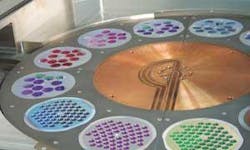
However, deposition of the same materials in the near-UV presents significant challenges. Refractory materials tend to have much higher absorption in the near-UV—so much so that oxides such as silicon, titanium, zirconium, and niobium are no longer useful. Problematic as well is the rapid change of the refractive index of materials in the near-UV, making it much more challenging to produce filters with high in-band transmission, deep out-of-band blocking, and sharp transitions between transmission and rejection. The relative thinness of coating layers required for high transmission in the UV only further complicates matters.
Despite these challenges, filters with unprecedented performance in the UV are being produced. Filters with transmission better than 80% in band, 10-6 out of band, and sharp transitions in between are enabling applications in spectroscopy, fluorescence microscopy, purification, sterilization, industrial processing, and semiconductor manufacturing.
Illumination source advances
None of this would be possible without the development of a multitude of light sources in the near-UV range. Previously, applications requiring UV illumination had fairly limited selections; xenon or deuterium for broadband output, mercury for quasi-monochromatic output, or a variety of laser sources (xenon chloride, xenon fluoride, third and fourth harmonics of Nd:YAG, nitrogen, helium cadmium, argon ion, to name a few) for true monochromatic output. Today, however, work being done to produce quasi-monochromatic and true monochromatic semiconductor light sources has created smaller, cheaper, and more energy-efficient sources of UV illumination.
Applications previously served by the quasi-monochromatic output of mercury arc lamps (with peaks at 253, 313, 334, 365, and 406 nm) are finding success using light-emitting diodes (LEDs) of gallium nitride (GaN), aluminum gallium nitride (AlGaN), and aluminum indium gallium nitride (AlInGaN). Commercial LEDs from these wide-bandgap III-V compounds are available with outputs as low as 280 nm, with tens of milliwatts of power, and thousands of hours of lifetime at room temperature. Applications for short-wavelength UV LEDs include biosensors, water purification, and fluorescence spectroscopy. For the more mature longer-wavelength UV LEDs (around 365 nm), the application space is more readily defined, and includes counterfeit detection, UV curing systems, photolithography, and DNA sequencing and analysis.
True monochromatic semiconductor light sources (laser diodes) in the near-UV are still a work in progress. Diodes at 375 nm with output power of tens of milliwatts and hundreds of hours are readily available commercially. Beyond those diodes, however, material limitations on the indium gallium nitride (InGaN) configuration make stimulated emission quite difficult.
All in all, developments in the near-UV spectrum are rapidly occurring. Standard optical components from lenses, mirrors, polarizers, and prisms, to more complex objectives and aspheres, are becoming more readily available. The aspheres and objectives, especially, enable the most efficient use of the UV illumination because they allow for smaller focused spot sizes—one of the key benefits of using UV light. Couple that advantage with filters produced through dense sputtering techniques that provide higher transmission and improved contrast, and it’s easy to see why applications across many industries are turning to the UV to solve their challenges and create a brighter, cleaner, safer, and healthier tomorrow for all of us.
About the Author
Gregg Fales
Senior Product Line Manager, Edmund Optics
Gregg Fales is senior product line manager, both at Edmund Optics (Barrington, NJ).