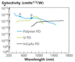
DETECTORS: Polymer photodetectors span the 300 to 1450 nm range
In September, Laser Focus World reported on quantum-dot-infused polymer photodetectors with responsivity from 300 to 1250 nm. Now, researchers at the University of California, Santa Barbara (UCSB; Santa Barbara, CA), CBrite (Goleta, CA), and South China University of Technology (Guangzhou, China) have extended the high end of the range up to 1450 nm by using a small-bandgap semiconducting polymer blended with a fullerene derivative.1 The broadband device operates at room temperature with dark-current and noise values well below those of narrowband inorganic-semiconductor detectors.
Typically, detectors based on gallium nitride (GaN), silicon (Si), and indium gallium arsenide (InGaAs) are used for sensing from 0.25 to 0.40 µm (UV), 0.45 to 0.80 µm (visible), and 0.90 to 1.7 µm (near-IR), respectively, with detectivities on the order of 1012 Jones (1 Jones = 1 cm Hz1/2/W) for room-temperature Si and cooled InGaAs detectors. Replacing multiple narrowband detectors with a single broadband detector would obviously have numerous benefits for a wide range of applications, including imaging, communications, environmental monitoring, and chemical/biological sensing.
Building on previous research that demonstrated ultrafast photoinduced electron transfer from semiconducting polymers to fullerenes to produce polymer photodetectors (PPDs) with fast temporal response and high sensitivity from 400 to 900 nm, the researchers developed a new polymer material blend with a molecular structure able to extend detectivity beyond 900 nm. The team experimented with a small-bandgap conjugated polymer called PDDTT, blended or layered with a methyl ester called PC60BM.
Optimizing HOMO and LUMO levels
Analysis of the highest occupied molecular orbital (HOMO) and lowest unoccupied molecular orbital (LUMO) levels of PDDTT and PC60BM shows that charge-separated carriers are efficiently generated by photoinduced electron transfer and transported to opposite electrode layers fabricated next to the polymer layers. For these fabricated devices, dark current is limited by the energy difference between the HOMO of PDDTT and the LUMO of PC60BM. To minimize the dark current, various PPDs were fabricated with different polymer multilayer structures and various combinations of blocking electrodes to suppress the thermally generated dark current.
Of the various devices fabricated with different combinations of PDDTT, PC60BM, and other polymer materials such as PEDOT layered between either indium tin oxide (ITO) or aluminum (Al) electrode layers, devices fabricated with PDDTT:PC60BM heterojunctions showed significantly better photoinduced charge transfer with long-lived mobile carriers compared to other polymer combinations. The best device (highest photocurrent, lowest dark current, and highest detectivity) was an ITO/PEDOT/PS-TPD-PFCB/PDDTT:PC60BM/C60/Al structure. In addition, PDDTT was found to be a promising semiconducting polymer for bulk heterojunction solar cells due to its high absorption coefficient over a broad absorption spectrum—nearly covering the entire solar emission spectrum.
A comparison of these various PPD devices against Si and InGaAs photodetectors showed that optimized PPDs had a spectral response from 300 to 1450 nm with a detectivity greater than 1013 Jones between 300 and 1150 nm and better than 1012 Jones from 1150 to 1450 nm (see figure). Not only do the PPDs operate over a broader wavelength range and display better detectivity than competing inorganic photodetectors, but the best devices also have a linear dynamic range (photosensitivity linearity) of 100 dB—close to that of a Si photodetector (120 dB) and better than an InGaAs detector (66 dB).
“The demonstration of such high-performance photodetectors fabricated with semiconducting polymers is another step toward the goal of replacing inorganic semiconductors with low-cost printable electronic devices in a variety of applications,” says Alan J. Heeger, UCSB professor and researcher.
REFERENCE
- Xiong Gong et al., Science Express online 10.1126/science.1176706 (August 13, 2009).
About the Author

Gail Overton
Senior Editor (2004-2020)
Gail has more than 30 years of engineering, marketing, product management, and editorial experience in the photonics and optical communications industry. Before joining the staff at Laser Focus World in 2004, she held many product management and product marketing roles in the fiber-optics industry, most notably at Hughes (El Segundo, CA), GTE Labs (Waltham, MA), Corning (Corning, NY), Photon Kinetics (Beaverton, OR), and Newport Corporation (Irvine, CA). During her marketing career, Gail published articles in WDM Solutions and Sensors magazine and traveled internationally to conduct product and sales training. Gail received her BS degree in physics, with an emphasis in optics, from San Diego State University in San Diego, CA in May 1986.
