NANOSCALE METROLOGY: Scatterfield optical imaging enables sub-10 nm dimensional metrology
RICHARD M. SILVER
Scatterfield optical imaging is a new technique that makes possible high-throughput measurement of sub-10 nm features using advanced, low-cost optical methods. It has the potential to substantially impact manufacturing productivity and process control, and to provide the measurement basis for new calibration standards well beyond the current state of the art. Researchers are developing this technique as part of the Advanced Optics Initiative of the Next Generation Nanometrology Program at the National Institute of Standards and Technology (NIST).1 The ultimate goal of this work is development of a high throughput measurement technique capable of imaging sub-10 nm features with sensitivity to nanometer-scale geometrical changes.
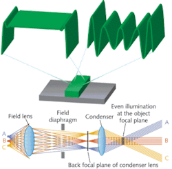
The ability to measure linewidth, feature overlay, and defects in nanoelectronic devices as small as 5 nm represents a factor of 50 extension beyond the practical Rayleigh limits of traditional visible-light microscopy. It is essential in this methodology not to be limited by conventional image-based edge-detection microscopy (see Fig. 1, top).
Scatterfield optical imaging technology enables two primary implementations–static and scanned illumination–both of which are based on similar optical platforms. In both cases, the optical design involves Kohler illumination, a configuration wherein each point of the illumination back focal plane maps to a plane wave of illumination (see Fig. 1, bottom). In most such systems the back focal plane is physically located inside the objective, and a set of relay optics is used to create a magnified conjugate back focal plane (CBFP). This CBFP is the location where the illumination angle, state of polarization, intensity distribution, and phase can be engineered.
The scatterfield technique uses similar engineering methods for both the collection and illumination paths. In the former, apertures and intensity control at the Fourier plane enable sophisticated control of the scattered electromagnetic fields. Thus, only selected components of the scattered fields can be viewed and analyzed. These methods can often be further enhanced using targets designed to optimize the optical response or sensitivity to a process to be controlled. The basic concept of using arrayed targets can fundamentally change the measurement physics, resulting in greatly enhanced sensitivity.
When this optical configuration is combined with high-speed signal processing, high-resolution CCD array technology, and reliable theoretical scattering models, it makes possible optical imaging and metrology with resolution well beyond the wavelength. This new microscopy method enables a significant leap in the sensitivity to geometrical changes of the sample on the order of one nanometer or better. Simulations indicate that it is reasonable to image features smaller than 10 nm with sensitivity to nanometer geometrical changes using optical microscopy.
Accuracy is key
A key enabling technology for these improvements is the unprecedented accuracy by which we can now calculate the electromagnetic scatter from features. With essential advances in optical-system characterization and profile normalization, it is possible to achieve previously unobtainable theory-to-experiment agreement. This enables both measurement accuracy of subresolution features and sensitivity to changes in geometry–something that has eluded optical scientists and semiconductor metrology experts for years.
The exact profile of the scattered field is extremely sensitive to small changes in the shape and size of the scattering feature. Once it is possible to accurately calculate the scattering function and propagate it through the optical system, it also becomes possible to measure features near to nanometer dimensions with nanoscale accuracy.
One important development in extending optical techniques is the accurate characterization of the optical instrument itself. A characterization method enabled by the scatterfield technique is that we can analyze the optical instrument as a function of illumination angle and polarization, thereby characterizing the optical path independently for each isolated angle of illumination. Comprehensive characterization is essential for accurate modeling of optical measurements. The illumination errors are mapped to a functional dependence that can be used as an input to the electromagnetic simulation tools, or alternatively to normalize various instrumentation effects in the experimental data for subsequent accurate comparison between experimental results and modeling outputs. This is an important step in improving optical model-to-experiment agreement.
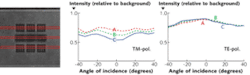
The procedure used to characterize the optical train captures a variety of errors including source inhomogeneity, angle-dependent transmission errors, and transmission errors as a function of polarization. It also measures system glare and background scatter, and carefully characterizes the CCD. These data are acquired in such a way as to allow separation of the illumination path and collection path errors. The resulting instrument function is then used to normalize data acquired by the CCD. The reflectivity results can be accurately normalized to either a known silicon reflectivity curve or a dielectric mirror to obtain an absolute instrument normalization function (see Fig. 2).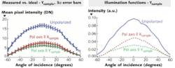
Method in action
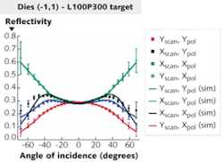
The method can be applied to measurement on an array of silicon lines. To illustrate, consider a single 300 mm wafer, fabricated by Sematech, with a focus exposure matrix having arrays of lines with linewidths that vary from die to die. Engineers completed reference metrology using a commercial critical dimension atomic-force microscope (AFM), measuring linewidth, sidewall geometry, line height, and pitch. All measurements were reported with 3σ uncertainties.
The engineers performed optical measurements on each of nine line arrays having dimensions that varied target to target by as little as 1 nm. They performed these measurements by capturing an image at each angle of illumination as the illumination was stepped across the x and y axes. They then determined a mean intensity per pixel and plotted that versus angle and polarization. The pitch (combined line and space) of the lines was nominally 300 nm, and a 450 nm wavelength light was used, resulting in only zero-order light reflected. Thus, a conventional image of a target is a constant intensity across the image field with no higher order optical content. These data show nanometer sensitivity to changes in linewidth based on the reference metrology numbers provided by the AFM (see Fig. 3).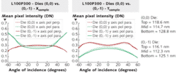
Additional recent research has used these methods to tailor or structure the incident illumination field to contain specific spatial-frequency components needed to best resolve the objects being observed. Complex scattering profiles or “signatures” can be enhanced in a fundamental way by controlling the spatial-frequency content in both the illumination and collection optical paths. When combined with sample design, the metrologist can begin to control the resulting scattered intensity profiles and imaging characteristics.
In the end
The methods described here have applications in the semiconductor and nanomanufacturing industries, as well as core applications in measurements for standards. The ultimate performance of these methods can be enhanced by using shorter measurement wavelengths. To address this, a new optical instrument, in the final stages of development, uses a 193 nm laser wavelength with full illumination and collection path engineering. This instrument, combined with complex parametric analysis, is expected to provide measurement and process-control solutions on some of the most challenging targets at the nanometer scale.
Acknowledgements
The author wishes to acknowledge Bryan Barnes for significant contributions to the data acquisition and analysis–as well as Mike Stocker and Ravikirran Attota. Thomas Germer and Alan Heckert, who helped with development of the RCW models and parametric analysis techniques, are also gratefully acknowledged.
REFERENCES
- R.M. Silver, B. Barnes, R. Attota, J. Jun, M. Stocker, E. Marx, and H. Patrick., Appl. Optics 46(20) p. 4248 (July 2007).
Richard M. Silver is a physicist in the Nanoscale Metrology Group of the Precision Engineering Division, one of five divisions of the Manufacturing Engineering Laboratory at the National Institute of Standards and Technology (NIST), Gaithersburg, MD; e-mail: [email protected]; www.nist.gov.