ORGANIC SEMICONDUCTOR SOURCES: Hybrid OLEDs combine vapor deposition with solution processing

ULRICH DENKER
Current organic-light-emitting-diode (OLED) device performance meets or exceeds the requirements for display applications. In this environment, the development focus changes from performance improvement to optimizing the manufacturing process. To produce cost-competitive OLEDs using current materials and processes, one option is to combine different approaches to OLED manufacturing. While OLEDs are traditionally produced using ultra-high-vacuum vapor deposition or solution processing, a hybrid device combines both methods. At first glance, this would seem to make OLED production more complicated, but there are a number of advantages in using this methodology.
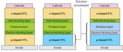
The typical layer sequence of an OLED using Novaled’s PIN structurea p-i-n sandwich of a p-doped layer, an insulator, and an n-doped layerstarts at the bottom with an inorganic anode that is usually made from indium tin oxide, or ITO (see Fig. 1). The organic layer stack consists of a doped hole-transport layer (HTL), blocking layers around the central light-emitting layer, and is finished by a doped electron-transport layer (ETL). The cathode is typically made from an inorganic material such as silver.
Redox (reduction-oxidation) doping of organic transport layers with molecular dopants offers several advantages including low driving voltages, wide choice of materials for cathode and anode, and good power efficiency.1 Novaled’s redox doping transport materials have long been used successfully for OLEDs in which all layers were deposited using vapor thermal evaporation (VTE). Recently, we investigated OLEDs in which some layers were deposited using solution processing. These hybrid OLEDs fall into two main categories: OLEDs in which only one layer is deposited by solution processing and the subsequent OLED stack is deposited in vacuum, and OLEDs that have multiple solution-processed layers with only the final layer stack deposited in vacuum. Both approaches have specific advantages and challenges.
OLEDs with a single solution-processed layer
The simplest approach for a hybrid OLED is to introduce a single solution-processed layer. A solution-processed HTL has the distinct advantage that the substrate is better planarized than with a vapor-deposited HTL. Films formed from solution generally have better surface-smoothing properties than vacuum-deposited layers. It is also possible to coat very thick layers in one step from solution by changing solution formulation. In a vacuum-thermal-evaporation process, on the other hand, the maximum deposition speed restricts the feasible layer thickness. The deposition speed can only be tuned in a limited range, otherwise the evaporation temperature will become too high and the organic material will be damaged.
Thick organic layers fabricated with a solution-processing step are useful on rough substrates when the inorganic anode material is not sufficiently smooth for the fabrication of good-quality OLEDs. In display applications, OLEDs are typically deposited on top of a backplane-driving circuit that forms a textured surface, making a smooth, solution-processed layer advantageous. The high conductivity of the Novaled p-doped layer enables layer thicknesses of several hundred nanometers without significant impact on driving voltages and OLED performance. Furthermore, the use of a solution-processed layer prevents pin-holes that can cause leakage currents and accelerate device degradation.
For hybrid OLEDs with a solution-processed HTL, we used the small-molecular host material NHT-5 and the small-molecular p-dopant NDP-2. These materials are stored as solids and dissolved in organic solvents before use. The use of organic solvents creates a water-free and non-acidic solution that is beneficial for applications in which the high boiling point and chemical properties of water pose a problem.
In the first step, the film-forming properties and conductivities of the solution-processed layers were studied and compared to vapor-deposited layers. Thin films of NHT-5 doped with NDP-2 with an approximate 100 nm thickness were formed by VTE or solution processing onto glass substrates with structured ITO contacts. Solution processing was performed by spin coating. The concentration of dopant in the layer was varied by co-evaporation for VTE or by the formulation of the solution for spin coating. Conductivity can be adjusted by doping concentration over several orders of magnitude (see Fig. 2). Higher conductivity is observed for solution-processed layers that can be interpreted by different morphology of the final layer depending on the process applied.
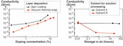
The molecular p-dopant NDP-2 is soluble in a variety of solvents. However, not every solvent that possesses the required solubility can be applied. Film-forming properties, solubility of the host material, compatibility with neighboring layers, and stability of the solution needs to be considered. The stability of solutions of NHT-5 and NDP-2 when stored in air was also tested. The tested solutions had 5%-by-weight solid contents of NHT-5 and NDP-2 in a ratio of 99:1, respectively. After storage of solutions in ambient atmosphere, thin films of NHT-5 doped with 1% of NDP-2 were spin-coated and dried. Conductivity measurements showed that solvent selection has a critical influence on the stability of a doped solution. Using some solvents, the solution is stable for at least several days, allowing preparation of larger quantities in one batch if required.
Because the properties of the solution-processed layers were very promising, complete hybrid OLEDs were fabricated. After spin-coating of the HTL, the OLEDs were transferred into vacuum and subsequent deposition of the following layers was done by VTE. Using this single-layer hybrid approach, the device yield was improved compared to a reference sample that was completely vapor deposited. Because the finished film has the same optical properties as a vapor-deposited layer, there is no need for extensive reoptimization if a vapor-deposited HTL is replaced by a solution-processed HTL in an OLED layer stack.
OLEDs with multiple solution-processed layers
For the example discussed in the previous section, the solution-processed layer is a small-molecule material and has only hole-transporting properties. If polymer materials are used, functional groups with hole-transporting and light-emitting properties can be added to the polymer and, in principle, a single-solution-processed-layer hybrid OLED can be fabricated in which only the electron-transport layers are deposited in vacuum.
In general, polymeric OLEDs also contain several solution-processed layers, imposing stringent requirements on the materials used. If a layer stack is fabricated by solution processing, it is imperative that a finished layer is not attacked and dissolved by subsequent coating steps. This can be achieved by using orthogonal solvents for each layer or by making the deposited film insoluble through a subsequent cross-linking step. Since cross-linking steps require high temperatures and can lead to unwanted diffusion of material, a fully solution-processed OLED with good performance is very difficult to obtain.
A hybrid device made from polymeric and small-molecule OLED materials can combine the advantages of both material classes. In one possible production process for such a device, the OLED stack, up to the light-emitting layers, is made from solution-processable materials (see Fig. 3). This enables the use of ink-jet-like printing methods for the formation of red/green/blue subpixels for producing large substrate sizes with high resolution, avoiding the scaling issues encountered when using very high-resolution shadow masks for vapor deposition. On top of the solution-processed light-emitting layers, organic electron-transport layers are deposited in vacuum together with the final metal cathode. By contacting several subpixels with one cathode, the resolution and alignment requirements are considerably relaxed.
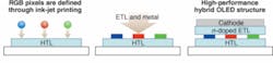
Use of a doped organic ETL enables a far wider choice of materials for the metal contact. In addition, it is possible to maximize the light output from the OLED layer stack by tuning the doped ETL thickness such that the distance between emissive layer and metal contact forms an optimal cavity inside the OLED. Because the metal needs to be deposited in vacuum anyway, the added process complexity is small.
REFERENCE
1. K. Walzer et al., Chemical Reviews 107, 1233 (2007).
Tell us what you think about this article. Send an e-mail to [email protected].
ULRICH DENKER is a physicist at Novaled, Tatzberg 49, 01307 Dresden, Germany; e-mail: [email protected]; www.novaled.com.