OPTOELECTRONIC APPLICATIONS: MICROPROCESSING - Ultrafast fiber lasers forge new microprocessing frontiers

Ultrafast fiber lasers are gradually displacing solid-state lasers for many scribing, marking, and nanopatterning applications in precision microprocessing and in transparent materials for displays, telecommunications, and even for silicon and thin-film solar photovoltaics. Unlike laser “materials processing,” which generally refers to cutting and welding applications on the macro scale (automotive welding, bulk glass and metal cutting), laser “microprocessing,” which involves high-power picosecond and femtosecond solid-state and fiber lasers, refers to microelectronics and semiconductor processing on the “micron” scale or smaller. Although solid-state lasers will continue to play a role in microprocessing, fiber lasers that offer high repetition rate (hundreds of kilohertz to megahertz range), high peak power, and moderate pulse energy continue to get noticed in the microprocessing community for their ability to improve the efficiency of ablation and material removal and modification, enabling a host of emerging applications.
One of the earliest and most well-known applications for femtosecond lasers was pioneered by IntraLase (Irvine, CA; now owned by Advanced Medical Optics) for cutting the corneal flap in laser-assisted in situ keratomileusis (LASIK) surgery using a fairly low-repetition-rate (10 kHz) diode-pumped solid-state Nd:YAG laser. But in early 2007, Carl Zeiss Meditec (Jena, Germany) announced its partnership with IMRA America (Ann Arbor, MI) in the launch of Carl Zeiss Meditec’s VisuMax system for laser keratome applications using what was hailed as an improved fiber-laser approach.
Silicon micromachining
VisuMax incorporates IMRA’s FCPA µJewel laser, which uses chirped-pulse amplification (CPA) in a large-core ytterbium (Yb)-fiber amplifier to deliver microjoule-level energy at 1 µm with 1 to 3 W average power at repetition rates from 100 kHz to 5 MHz—all without water cooling. “The ability to scale the power of our platform from 0.5 W for eye surgery up to 10 W means we can move beyond medical and low-power applications and cut thin silicon wafers for solid-state hard drives and flash memory at die strengths comparable to mechanical processes without the need for the post-process of laser dicing,” says Kiyomi Monro, director of business development for IMRA America.
“After demonstrating wafer singulation at greater than two times the die strength of UV-diced wafers, we are now working with a leading semiconductor company to explore singulation of silicon wafers,” says Monro. “When your pulse duration goes into the 500 fs regime, the material interaction is not necessary thermal. Ultrashort pulse machining is beneficial when you don’t want thermal interactions, which may weaken the strength of silicon dies and cause other problems.”
Scribing/marking/ablation
There are two distinctively different approaches to development of ultrafast lasers for micromachining applications. One is led by established companies historically involved in solid-state lasers such as Coherent (Santa Clara, CA) and Newport Spectra-Physics (Irvine, CA), while another is driven by relatively small companies focused on development of all-fiber (and smaller footprint) solutions, such as IMRA and Fianium (Southampton, England).
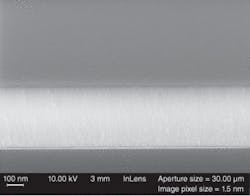
Fianium focuses on ultrafast applications but avoids the use of CPA methods, choosing instead to use all-fiber, direct amplification of picosecond pulses in a master-oscillator power-amplifier (MOPA) configuration. “We try to keep our lasers as simple and therefore as reliable as possible, relying on advanced fiber-amplifier development with ultralow nonlinearity to enable power and pulse-energy scaling,” says John Clowes, vice president of business development for Fianium. “Many microprocessing applications such as marking, scribing, and pulse laser deposition require quite modest pulse energies (up to 20 µJ) but at high repetition rates and average power (several megahertz and up to 50 W) to increase throughput (see Fig. 1). We’ve developed highly efficient fiber amplifiers that can deliver 10 to 20 µJ of pulse energy for 10 to 20 ps without the use of chirped pulse amplification. The quality of the amplified pulses also means that they can be efficiently compressed to the subpicosecond level at several microjoules of pulse energy for those niche applications such as bladeless LASIK in which picosecond systems cannot be used.”
Ultrafast fiber lasers hold a position in the market as seed oscillators and moderate-energy (up to 20 µJ) sources for applications ranging from scribing, advanced marking, pulsed laser deposition, and medical and refractive surgery. In addition, the high intensities, excellent beam quality, and scalable powers make ultrafast fiber lasers ideally suited for efficient, multiwatt harmonic generation. High repetition rates (up to several hundreds of megahertz), quasi-CW Green (532 nm), and UV (355 and 266 nm) sources have established applications in manufacturingtrimming, polymer processing, marking, and semiconductor wafer inspection. Nonetheless, the main challenge of pure ultrafast fiber lasers is to scale the energy level in the picosecond regime toward 100 µJ for applications requiring higher energy removal, including drilling, dicing, and cutting.
Higher-pulse-energy applications
The definition of “ultrashort” in the thermal argument is not limited to femtosecond pulse operation. For longer pulses in the nanosecond range, material is “boiled off” or removed by thermal means. But for picosecond and faster pulses, multiphoton absorption essentially breaks the chemical bonds within a material in a cold ablative process; essentially, picosecond IR pulses can deliver spatial resolution comparable to a nanosecond UV laser. In response to the growing need for “ruggedized” lasers to process metal and ceramic materials, as well as silicon, some companies have started to use a solid-state/optical-fiber “hybrid” approach to produce high-peak-power and high-average-power picosecond pulses.
Coherent released Talisker—available in 1064, 532, and 355 nm wavelengths—in a hybrid design using a modelocked fiber laser oscillator whose output is boosted by a free-space amplifier to deliver 15 ps pulse widths with 100 µJ pulse energy at a repetition rate up to 200 kHz. “Over the past 10 years or so, researchers in the microprocessing field have determined the ‘sweet spot’ for ultrafast lasers—the specific combination of pulse energy, pulse repetition rate, and other parameters that produce the best results for a variety of microprocessing applications,” says Matthias Schulze, director of technical marketing for Coherent. “We have been carefully following this research and came to the realization that our customers would benefit most from the ruggedness and precision of an ultrafast fiber laser combined with the higher pulse energy enabled by free-space amplification.”
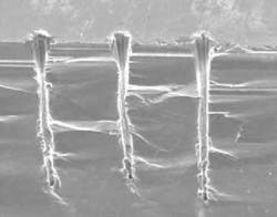
Coherent has explored the use of Talisker for silicon-through-via (STV) drilling using both percussion (laser spot size matches the silicon via or hole diameter) and trepanning (small spot cuts the hole by scanning in a circular pattern) methods (see Fig. 2). Because experiments show that the attainable hole depth falls off dramatically for larger spot sizes, the key to deeper vias is using small spot sizes of approximately 10 μm. With this spot size, holes as deep as 200 µm and 5 to 15 µm wide can be drilled with as few as 10 pulses at pulse energies of less than 25 μJ for a drilling rate of 1500 to 1800 vias/s.Thin-film removal and machining
Newport Spectra-Physics introduced its picosecond “hybrid” Pantera laser at Laser 2007 in Munich, Germany, to address applications in cutting, ablation, or structuring of thin layers. “Nanosecond lasers often create liquid droplets of debris when ablating material,” says Michael Kauf, marketing and business-development manager for Newport’s Fiber Laser Business Group. “These droplets either adhere to the edge of a hole or feature and create a crater or they fall back and melt to the surface, compromising surface quality. In contrast, picosecond machining with a laser like Pantera creates much finer debris that falls back to the surface as a fine dust and can be easily wiped off.”
Composed of a conventional oscillator and fiber amplifier, Pantera’s 50 W infrared (IR) beam can be subsequently converted into 30 W of green and 12 W of UV power. At these power levels, typical uses include cutting of dielectric and isolation material for flexible printed-circuit boards and die stacking. Examples include cutting 75-µm-thick polyimide at 1 m/s by directing the beam to the workpiece using scanner optics. Because there is no sign of thermal damage even at this thickness, the cutting can be increased to 4 m/s for 25-µm-thick polyimide. Other uses include ablating and structuring of transparent conductive oxides on flat-panel displays and thin-film solar cells. While these thin layers can be machined with nanosecond lasers, the throughput is often limited because of the repetition rate of the laser, not the laser power.
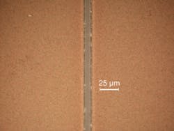
When Pantera is operated at 12 W, 355 nm, and a repetition rate of 80 MHz, its UV power allows extreme processing rates of multiple meters per second when machining thin layers. For example, Pantera can remove and precisely pattern 1-µm-thick layers of indium tin oxide (ITO) on a glass substrate at a processing speed of 25 m/s without substrate damage (see Fig. 3).Coherent’s Talisker has also been evaluated in the removal of thin films such as ITO and thin (tens of nanometers) metal films on plastic and glass substrates that are patterned for RFID cards and disposable medical sensors. A Talisker operating at 1064 nm with 1 µJ pulses in a 20 µm focused spot size successfully removed a 20-nm-thick aluminum film from a glass substrate at a scan rate of 3 m/s with negligible impact to the underlying substrate. “Pulse energy determines the maximum depth that you can drill, cut, or scribe,” says Schulze. “Very high-repetition-rate and lower-pulse-energy lasers can cut thin materials, but are problematic for thicker materials. Megahertz-speed ultrafast lasers must often be reduced to kilohertz operation to keep up with the scanning galvanometers being used; otherwise, once you’re done cutting, the laser dwells on the substrate and produces heat.”
Emerging applications
Coherent has also evaluated its picosecond hybrid laser for machining glass in microfluidic (lab-on-a-chip) applications, as well as for machining next-generation stents made of polylactide or other similar polymer materials to ensure a smooth surface and prevent the buildup of scar tissue on the stent that can defeat its purpose in keeping blood vessels clear.
Whether the ultrafast laser operates at picosecond or femtosecond speeds, there is no doubt that many applications haven’t yet been envisioned. “It’s a chicken and egg situation,” says Schulze. “Lasers are developed today for many known applications; however, ultrafast fiber-based lasers will no doubt have an ever-bigger footprint for micromachining and even future nanomachining applications—we’ve only just scratched the surface regarding what these lasers can do.”
Additional Resources
For additional information please see the Clark-MXR Micromachining Handbook at www.cmxr.com/industrial/handbook/index.htm.
About the Author

Gail Overton
Senior Editor (2004-2020)
Gail has more than 30 years of engineering, marketing, product management, and editorial experience in the photonics and optical communications industry. Before joining the staff at Laser Focus World in 2004, she held many product management and product marketing roles in the fiber-optics industry, most notably at Hughes (El Segundo, CA), GTE Labs (Waltham, MA), Corning (Corning, NY), Photon Kinetics (Beaverton, OR), and Newport Corporation (Irvine, CA). During her marketing career, Gail published articles in WDM Solutions and Sensors magazine and traveled internationally to conduct product and sales training. Gail received her BS degree in physics, with an emphasis in optics, from San Diego State University in San Diego, CA in May 1986.

