CMOS Detectors: Scientific monolithic CMOS imagers come of age

Complementary metal-oxide semiconductor image-sensor technology has displaced charge-coupled-device technology in many commercial applications and is now moving to capture high-performance custom markets.
JAMES JANESICK, TOM ELLIOTT, AND JOHN TOWER
Imagers based on monolithic complementary metal-oxide semiconductors (CMOS) were first introduced as a competitor to charge-coupled-device (CCD) detectors more than a dozen years ago. Although CMOS has been commercially successful along the way (most notably in cell-phone and digital cameras), there has been little interest from the scientific-imaging community in applying the new sensordespite the fact that its low cost, low power consumption, high level of on-chip system integration, high video throughput, fast readout of selective regions, and long-lived radiation tolerance obviously trump the benefits of the CCD. The simple explanation for the lack of scientific enthusiasm is that, historically, CMOS imagers have been severely deficient in performance when compared to the CCD.
Technically, a few design groups have recognized this dilemma: that “standard” CMOS fabrication processes cannot fundamentally produce a high-performance imager. Instead, custom manufacturing schemes similar to those used by the CCD are required. Only recently have we seen the implementation of scientific designs that demonstrate the ability of CMOS to perform just as well, if not better, than CCDs. This breakthrough now opens CMOS technology to a wide range of new scientific applications beyond CCD limitations.
Defining high performance
Several key parameters define when an imager can truly claim “high performance.” The ability of incident photons to generate useful signal charge, for example, depends on a sensor’s quantum efficiency (QE). As CCDs demonstrated more than three decades ago, rear illumination optimally yields the highest QE possible for any imager (with 1 to 11,000 Å wavelength coverage). Following suit, scientific back-illuminated (BI) CMOS imagers are currently achieving similar QE performance. However, to do the job correctly, near-infrared and soft-x-ray photons require thick silicon (more than 50 μm) for efficient absorption characteristics.
In contrast, commercial CMOS imagers typically provide a photoactive thickness of only 1 to 3 µm intended for visible-light imagery (400 to 650 nm) in which photon absorption length is short in silicon. To efficiently collect charges generated deep within the silicon, without pixel crosstalk and consequential blurring, high-resistivity epitaxial silicon is essential. In addition, an old CCD technique that uses a high-voltage “substrate bias” must sometimes be used to generate deep electric fields for very thick CMOS sensors (referred to as “deep depletion imagers”).
Charge-transfer efficiency (CTE)the ability for signal charge to be transferred from a photo region to a readout amplifieris also a parameter of critical imager performance. State-of-the-art, charge-coupled CMOS pixels exhibit better than 99.5% CTE for low signal levels of less than 20 electrons (e-). Interestingly, this high CTE can be maintained when a CMOS imager is subjected to high (1 M rad) radiation damage environments, such as in aerospace applications. This important attribute is a remarkable CMOS feature because CCD imagers stop working at considerably lower dose levels. As it turns out, radiation damage is the Achilles heel of CCDs, given that thousands of transfers are typically required to move signal charge to the on-chip amplifier, resulting in “image lag” when silicon is damaged by high-energy radiation sources. In contrast, CMOS only involves a single transfer because pixels are addressed directly, producing a technology insensitive to radiation-induced deferred-charge CTE issues.
Reducing CMOS read noise
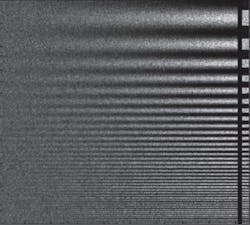
Until recently, CMOS imagers have exhibited significantly higher read noise than slow-scan scientific CCDs, which routinely achieve 1 to 2 e- root-mean-squared (rms). Today, custom CMOS imagers show an equivalent noise level achieved by using innovative signal processing schemes and pixel designs with high voltage-to-electron (V/e-) conversion efficiency. For example, a 479 × 476 test sinusoidal contrast target image taken by a CMOS imager that incorporates five-transistor (5T) charge-coupled pixels can exhibit a 2 e- noise performance (see Fig. 1). The light level on the sensor is adjusted to generate an average signal of 18 e- with a corresponding photon shot noise of 4.2 e-. Contrast signal-to-noise-ratio (S/N) performance varies (from left to right) linearly from approximately 0 to 3 in the image.
Although noise floors lower than 2 e- will not significantly improve S/N for extended images because of photon shot noise, some scientific applications will benefit greatly from the reduction (such as single-photon counting and associated energy measurement). X-ray testing represents an acid diagnostic test for imagers because charge collection efficiency (CCE), read noise, CTE, and QE performance must be ideal to generate a respectable response; commercial CMOS sensors usually fail this test outright. A basalt x-ray histogram taken with a custom 15-µm-thick BI CMOS array in response to a Fe-55 fluorescing (5.9 keV) x-ray source (the strong K-α line indicated is off scale to show the weaker x-ray lines) shows good separation between x-ray linesmost notably the Fe-55 K-α (1613 e-) and K-β (1780 e-) lines (see Fig. 2).
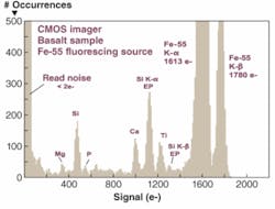
The ability to distinguish weaker lines in x-ray testing is limited by the sensor’s read noise and the “Fano noise” generated by x-rays. The response presented here is the first time a CMOS imager has clearly resolved x-ray lines and is considered “Fano noise limited” over the soft-x-ray 100 to 10 keV photon-energy range (a figure of merit originally used by CCDs when the sensor’s read noise is negligible compared to Fano noise). Reducing noise further to the subelectron level would allow CMOS to work as an imaging spectrometer in the 10 to 100 eV extreme-UV range.
Fundamentally, CMOS read noise is limited by random telegraph signal (RTS) noise and background flicker noise associated with surface states in output metal-oxide-semiconductor field-effect-transistor (MOSFET) pixel amplifiers. These noise sources can be reduced considerably with the old CCD invention of using buried channel MOSFETs to curtail bias-current surface interaction. This technology will undoubtedly produce a subelectron noise floor in the very near future, thus surpassing CCD read noise.
In addition, increasing the V/e- conversion gain will further reduce noise proportionally. For example, the 2 e- noise floor demonstrated by the 5T CMOS imager described previously is generated by 50 µV/e- pixels. The conversion gain can be made as high as 200 µV/e- with 0.18 µm CMOS design rules to reduce parasitic or subfemtofarad sense capacitance.
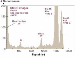
Finally, CMOS, like CCD, can use nondestructive readout schemes in which multiple samples are taken and averaged together to reduce the read-noise floor. This technique has already proved successful in the lab by achieving subelectron performance to the level at which the first signs of individual visible photoelectrons have been detected. It is also important to mention that read noise, as with CTE performance, is insensitive to radiation damage for CMOS pixels (see Fig. 3).
Faster frame rates
A distinguishing CMOS feature is its natural ability to work at very fast frame rates while preserving very low read noisesomething that CCDs cannot do easily. A CMOS imager accomplishes this task by reading every column in a given row simultaneously (parallel readout) whereas the CCD inherently reads signal charge one pixel at a time (serial readout). Parallel readout allows sufficient signal processing and settling time (typically a few microseconds given per row) to achieve low noise while at the same time performing fast parallel multiplexing and frame readout. Additional speed is achieved through reading the top and bottom portions (or multiple vertical subregions) of the imager together.
With this architecture, state-of-the-art 1500 × 1500-pixel BI CMOS monolithic imagers are actively being designed for scientific applications with expected read-noise performance of less than 2 e- at 1000 frames per second (fps) readout, generating an effective output pixel rate of 2.25 gigapixels/s. On-chip analog-to-digital converters (ADCs) are incorporated to reduce off-chip support electronics to a minimum.
Breaking CMOS barriers
It is still difficult for CMOS to compete with the CCD on a few performance parameters. Two popular parameters in which CMOS occasionally lacks are charge-handling capacity and linearity performance. Both parameters are fundamentally limited by the amount of signal swing that takes place within a pixel. A CMOS detector’s operating potentials are inherently lower compared to higher voltages used by CCDs. Therefore, CMOS has more trouble meeting full well and nonlinearity requirements than does the CCD. However, many tricks are available to partially beat these problems, if necessary. For example, 0.18 µm CMOS fabrication processes allow high-voltage 5 V analog pixel circuitry to be mixed with low voltage 1.8/3.3 V digital logic designs. Also, operationally CMOS pixels can double sample the video under two different V/e- conversion conditions. The first sample is taken using a high-V/e- state to encode read noise, while the second sample is taken immediately after V/e- is rapidly lowered to encode full well. The V/e- value is physically reduced by incorporating additional sense capacitance into each pixel (typically above the photo region for a BI device). This encoding scheme is primarily suited for large pixels (more than 12 µm) that require a large dynamic range.
Pixel size, array size, and cost are also important characteristics for high-performance scientific imagers. The smallest pixel with reasonable performance that compares to a high-performance CCD pixel is approximately 8 µm. Larger pixels up to 25 µm are possible while still maintaining low read noise. A CMOS detector’s array size is limited to approximately a 22 × 22 mm step-and-repeat field printed on 200 mm silicon wafers (scientific CCDs are usually fabricated on 150 mm wafers using full-projection printing allowing full wafer-scale imagers). For larger CMOS imagers, an expensive “stitching” process must be used.
Although initial fabrication investment for CMOS is considerably more expensive than CCD (because approximately two-dozen costly 200 mm reticule sets are required in the lithography process), CMOS becomes less and less expensive as the quantity of wafers fabricated increases.
Without a doubt, developments over the last few years indicate that CMOS imaging applications will be very active in the future. Nearly 40 years ago, the CCD began to compete with photographic film and proceeded to assume all commercial and scientific applications. Through these new developments in scientific CMOS imaging, we may witness another “imager revolution.”
Tell us what you think about this article. Send an e-mail to [email protected]
JAMES JANESICK is manager, Advanced Sensors Group at Sarnoff, 4952 Warner Ave., Suite 300, Huntington Beach, CA 92649; e-mail: [email protected]. TOM ELLIOTT is principle engineer at the Jet Propulsion Laboratory, California Institute of Technology, 4800 Oak Grove Dr., Pasadena, CA 91109, and JOHN TOWER is technical director at Sarnoff, CN5300, 201 Washington Rd., Princeton, NJ 08543-5300; e-mail: [email protected]; www.sarnoff.com.