DISPLAY OPTICS: Contact lens could create virtual display
Researchers at the University of Washington (Seattle, WA) have successfully embedded optoelectronic devices into a biocompatible contact lens. This achievement is a significant step toward enabling virtual head-up displays within the human eye, delivering visual aids to help vision-impaired individuals, or for incorporating biosensors directly on the surface of the eye, among many other possible applications.1 “Looking through a completed lens, you would see what the display is generating superimposed on the world outside,” said Babak Parviz, an assistant professor of electrical engineering. “This is a very small step toward that goal, but I think it’s extremely promising.”
Integrating the devices within the contact lens begins with a 100-µm-thick polyethylene terephthalate (PET) substrate that is used as a template for patterned electrical interconnects and later, optoelectronic devices such as light-emitting diodes (LEDs). The films are cut with a CO2 laser into standard 4 in. wafers for use in standard microfabrication equipment.
To create the electronic circuits, standard photolithography, metallization, and lift-off steps are performed on the resist-patterned wafers. The wafers are then baked and cut into contact-lens shapes again by a CO2 laser.
Demonstration of the incorporation of a representative optoelectronic component was accomplished with a red-emission micro-LED. Compound semiconductor multilayer structures were grown separately from the contact lens using metal organic chemical-vapor deposition to create circular LED structures with approximate 320 µm diameters. Building the active LED structures on a sacrificial aluminum arsenide layer allows them to be easily removed with a hydrofluoric acid etch and placed on the contact lenses as individual elements.
Using a self-assembly process, alloy bumps are placed on particular locations or assembly sites on the PET wafer and the LED microdevices are flowed in solution over the wafer and attach to the assembly sites. The LED devices have n and p contacts on the same side of the LED for activation by the electronic template patterned on the wafer. A final heating step melts and joins the LEDs to the template metal interconnects.
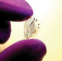
Finally, the contact lenses with optoelectronic elements are encapsulated with a polymethylmethacrylate (PMMA) coating to make them biocompatible with eye tissue. The lenses are then placed in an aluminum mold and baked to obtain the curvature of a contact lens (see figure).
The lenses were successfully tested on rabbits (without LED structures), and the LEDs were found to be operational when probed with electrical pulses, although yields during the final coating and lens-forming processes need to be improved. Eventually, the team hopes to power the lenses using a combination of radio-frequency signals and solar cells placed on the periphery of the contact lens surface so as to not obstruct vision of the wearer.
Although he acknowledges that the research to date is only a starting point, Babak Parviz adds, “Potential applications in gaming, augmented reality, mobile computing, and mobile telecommunication devices are tremendous for this technology. As we encourage other research groups to explore what might be possible when sophisticated functional electronics and optoelectronics are integrated into a contact lens, it is likely that many other applications will appear.”
REFERENCES
1. H. Ho et al., Proc. IEEE MEMS 2008, Fabrication ThP poster presentation, Tucson, AZ (January 17, 2008).
About the Author

Gail Overton
Senior Editor (2004-2020)
Gail has more than 30 years of engineering, marketing, product management, and editorial experience in the photonics and optical communications industry. Before joining the staff at Laser Focus World in 2004, she held many product management and product marketing roles in the fiber-optics industry, most notably at Hughes (El Segundo, CA), GTE Labs (Waltham, MA), Corning (Corning, NY), Photon Kinetics (Beaverton, OR), and Newport Corporation (Irvine, CA). During her marketing career, Gail published articles in WDM Solutions and Sensors magazine and traveled internationally to conduct product and sales training. Gail received her BS degree in physics, with an emphasis in optics, from San Diego State University in San Diego, CA in May 1986.