ULTRAFAST FIBER LASERS: Femtosecond fiber laser enables reliable wafer-level processing
LAWRENCE SHAH, KIYOMI MONRO, AND GYU C. CHO
Consumer microelectronics are continually moving toward higher-density interconnects in semiconductor chips and packages. The complexity of materials composition incorporated into the chips–processor and memory alike–requires a new level of package-processing technology. While conventional, mechanical wafer-singulation techniques dominate the industry, their applicability for dicing thin (less than 100 µm) semiconductor wafers is limited by the need to reduce cutting speed to achieve sufficiently high process yield. This problem is further complicated by reduction in the separation between die (street width) and by the increasing use of low-k dielectric insulating films, making conventional dicing methods only marginally suitable for next-generation integrated circuits.
Laser-based wafer-level singulation technology has been researched in the industry over the past decade to overcome the limitations of mechanical techniques. Ultraviolet (UV) nanosecond lasers have demonstrated the ability to scribe wafers with fragile back-end interconnects with greater throughput and improved reliability relative to mechanical methods. Nevertheless, thermal stress associated with nanosecond laser singulation reduces die breakage strength, thereby reducing final device lifetime and reliability.1 To address these issues, IMRA America has demonstrated an ultrashort-pulse fiber-laser system capable of achieving significant improvements in die break strength relative to other methods that is scalable to industrial requirements for throughput and overall cost (see Fig. 1).
Singulation challenges
Diode-pumped solid-state (DPSS) UV nanosecond laser systems have overcome semiconductor processing issues such as substrate chipping, small kerf width, and processing throughput. However, the thermal nature of nanosecond laser ablation causes a significant reduction in the die failure stress relative to mechanical dicing.
The failure stress of a die is given by σ(stress) = 3FL/2bh2, where F is the applied force, L is the span, b is the die width, and h is the die thickness (see Fig. 2). Using this measurement method, mechanically diced die typically have a failure stress of 650 MPa regardless of the direction of applied force. For UV nanosecond laser dicing, the failure stress reduces significantly to 440 MPa for the cut surface in compression and 200 MPa for the cut in tension. The differential between laser-cut die in compression or tension can be significantly reduced by using a three or four-point bend-test unit, in which case the failure stress is 250 MPa in compression and 174 MPa in tension; however, this is still less than half the value associated with mechanical dicing.2 While cutting speeds in excess of 100 mm/s enable high throughput and high die yield, the degradation of die failure stress significantly compromises subsequent device packaging and reduces overall device lifetime.It has been known for several years that ultrashort-pulse lasers can virtually eliminate thermal diffusion beyond the ablated region associated with nanosecond laser pulses.3 However, the improvements in cut quality typically come at the expense of dicing speed. Furthermore, these studies demonstrate that the cleanest cuts are achieved with relatively low laser fluence on target. For conventional Ti:sapphire-based femtosecond laser systems generating 1 mJ pulses at 1 kHz, the incident pulse energy must be significantly attenuated or the energy redistributed into a line focus. However, even under optimal conditions, 5 mm/s was the highest dicing speed achieved through 50-µm-thick silicon.4
Ultrashort-pulse advantages
For ultrafast lasers to be viable for wafer singulation, the technology must allow for scaling of laser repetition rate and average power. A fiber-based femtosecond amplifier is an excellent choice for these scalabilities. High optical gain and high slope efficiency enables high average power in a single path configuration with no need for regenerative amplification. This also allows the use of low-voltage, fiber-pigtailed acousto-optic modulators for repetition-rate selectivity. By doing so, a pulse repetition rate up to tens of megahertz is easily achieved.
Recently demonstrated nonlinear pulse compression has enabled IMRA America to realize fiber-chirped pulse amplification (FCPA) in a robust, compact package.5 The FCPA-based femtosecond laser has matured and provides the reliability and performance necessary for industrial applications. The large-core amplifier fiber provides single-transverse-mode output and is virtually insensitive to thermal lensing since beam propagation is defined by the waveguide nature of the fiber. Although the maximum achievable pulse energy is limited by nonlinear effects due to the small mode-field diameter within the fiber (typically less than 30 µm), the technology is capable of generating pulses with energies greater than 10 µJ and can be scaled to powers beyond 10 W in a compact package without water cooling.6
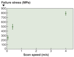
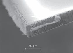
Failure stress measurements for 50-µm-thick silicon wafers as a function of scan speeds were analyzed using an FCPA µJewel series laser producing 10 µJ pulses of 700 fs duration at a pulse repetition rate of 500 kHz (see Fig. 3). To achieve a complete cut, the number of scan passes was proportional to the scan speed such that the average cutting speed was 6 mm/s in these experiments. Data confirmed that the best results are obtained using the highest scan speed. At 4 m/s scan speed, the failure stress (measured with the cut side in compression) exceeds that of mechanical dicing at 780 MPa. Reducing the scan speed to 400 mm/s causes the failure stress to fall below 500 MPa, roughly equivalent to that of UV nanosecond laser cutting. A failure stress of 253 MPa is measured when scan speed is reduced to 80 mm/s.Scanning-electron-micrograph (SEM) images also show that the appearance of the cut is greatly improved when scanning at 4 m/s relative to 80 mm/s. No post-processing or cleaning was implemented before the failure stress measurement and SEM imaging. Therefore, significant reduction in the amount and extent of ablation debris is another important benefit of scanning at high speed.
These results agree with the observation of thermally induced die strength for nanosecond laser systems. It is known that thermal accumulation can be significant for high-repetition-rate ultrashort-laser processing.7 To confirm that die strength and cut quality degradation also results from virtually instantaneous heat deposition, we repeated our singulation experiments at 4 m/s scan speed and a pulse repetition rate of 500 kHz using a pair of 10 µJ ultrashort laser pulses separated by 25 ns. Under these conditions, the die strength was reduced to 390 MPa. Likewise, the cut walls are rougher and more debris is evident on the sample surface (see Fig. 4). Consequently, it is not only necessary to manage the amount of heat deposited on nanosecond time scales when using an ultrashort laser pulse, but it is also necessary to properly choose the process parameters to avoid accumulative heating when scaling the laser repetition rate for increased throughput.The investigation of die break strength reveals significantly low heat effect when wafers are processed at high speed and high pulse repetition rate–a distinct advantage of a fiber-based laser. The results present the relevance and importance of femtosecond wafer-level processing in next-generation microelectronics device manufacturing.
REFERENCES
- J. Li et al., Proc. Electronic Components and Tech. Conf. 2007, p. 761 (May 29-June 1, 2007).
- L. Migliore, Proc. SPIE 6458 (2007).
- T. H. R. Crawford et al., Appl. Phys. A 80, 1717 (2005).
- H.K.Tönshoff et al., Third Int’l. Symposium on Laser Precision Microfabrication, Proc. SPIE 4830, 531 (2003).
- Z. Liu et al., Photonics West 2005 post-deadline paper (2005).
- L. Shah et al., Optics Exp. 13(12) 4717 (2005).
- S. Eaton et al., Optics Express 13(12) 4708 (2005).
LAWRENCE SHAH is a former research scientist in fiber laser applications at IMRA America and is currently a research scientist at The School of Optics/CREOL at the University of Central Florida, 4000 Central Florida Blvd., Bldg. 53, Orlando, FL 32816; www.creol.ucf.edu. KIYOMI MONRO is an advisor to IMRA America for the semiconductor market. GYU C. CHO is a VP responsible for technology and business development at IMRA America, 1044 Woodridge Ave., Ann Arbor, MI 48105; e-mail: [email protected]; www.imra.com.


