TERAHERTZ TECHNOLOGY: Black silicon emits terahertz radiation
Treating silicon with repeated high-energy laser pulses or through etching in a plasma creates nanosize structures on its surface, rendering the silicon black in color and able to absorb light and heat for potential use in solar cells and environmental sensors. Yet another use for black silicon has now been demonstrated by researchers at the Fraunhofer Gesellschaft (Munich, Germany), the Fraunhofer Institute for Physical Measurement Techniques IPM (Kaiserslautern, Germany), and Friedrich Schiller Universität (Jena, Germany): as an emitter of terahertz radiation.1
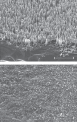
A 525-µm-thick black silicon sample was prepared on a clean, 2 to 10 Ω-cm silicon wafer in an inductively coupled plasma through reactive-ion etching for ten minutes using sulfur hexafluoride and oxygen. The process created 2-µm-high, 300-nm-diameter needles that were later damaged to confirm that the experimental results were indeed due to the needle structure of the black silicon (see figure). Black silicon offers very strong absorption of visible and infrared radiation, while the large penetration depth of this indirect semiconductor is effectively reduced to the submicron range under its surface by the needle structure, regardless of the path of the photons. The anisotropy shown by black silicon toward its surface causes a polarization effect that can create terahertz emission.
To quantify the emitted terahertz radiation, a time-domain spectroscopy setup used a 780 nm unfocused Ti:sapphire laser (2.5 W average power, 100 fs pulse duration, 750-µm-diameter beam) to illuminate the heat-sink-mounted black silicon emitter in both a quasi-transmission and a quasi-reflection geometry, meaning the pump laser illuminated the front side of the black silicon substrate at various angles of incidence to its normal (0° for normal incidence, 90° for grazing incidence) while the emitted radiation was detected from the back side of the substrate and the reflected radiation from the front side. The emitted radiation was detected by a low-temperature-grown gallium arsenide antenna with 20 µm dipole length.
Angles of maximum emission
In quasi-transmission, the black surface faces the laser and terahertz optics image the backside of the black silicon emitter onto the detector. In this case, maximum terahertz emission was observed close to grazing incidence, at approximately 70°, and no emission was observed for normal incidence. The presence of terahertz emission was reduced significantly when the black silicon surface was damaged, and was eliminated entirely when a polished silicon wafer was substituted in the measurement setup.
In quasi-reflection, maximum terahertz emission was observed at 45° incidence, and was comparable in characteristics to terahertz emission using indium arsenide (InAs). However, unlike InAs emitters, the terahertz amplitude was almost insensitive to the polarization state of the pump laser, resulting in improved absorption and increased terahertz emission.
The center wavelength of the generated terahertz radiation was around 600 GHz with a bandwidth extending from roughly 100 GHz to 2 THz. Although the generated output power in these experiments was much less than the terahertz power generated with standard materials, the black silicon was not optimized in terms of doping levels or surface preparation for maximum emission; this is the goal of future experiments.
“Usually, in indirect semiconductors the light absorbed creates electron hole pairs far from the surface,” says Patrick Hoyer, a researcher at the Fraunhofer Gesellschaft. “By using light-scattering processes of black silicon on the one hand and nanosize cavities within the material to pin the electronic bands to the surface on the other, a far larger part of the electron-hole pairs is created within the intrinsic electrical field of the semiconductor. Apparently, for this experiment, black silicon tends to behave more like a direct semiconductor. Further research using terahertz emission to characterize semiconductor materials will show the potential of black silicon for devices in the area of solar-energy conversion.”
REFERENCE
- P. Hoyer et al., Appl. Phys. Lett. 93, 091106 (Sept. 3, 2008).
About the Author

Gail Overton
Senior Editor (2004-2020)
Gail has more than 30 years of engineering, marketing, product management, and editorial experience in the photonics and optical communications industry. Before joining the staff at Laser Focus World in 2004, she held many product management and product marketing roles in the fiber-optics industry, most notably at Hughes (El Segundo, CA), GTE Labs (Waltham, MA), Corning (Corning, NY), Photon Kinetics (Beaverton, OR), and Newport Corporation (Irvine, CA). During her marketing career, Gail published articles in WDM Solutions and Sensors magazine and traveled internationally to conduct product and sales training. Gail received her BS degree in physics, with an emphasis in optics, from San Diego State University in San Diego, CA in May 1986.