GERMANIUM-ON-SILICON LASERS: Germanium lasers may help photonic integration with silicon
Germanium could be the key ingredient needed to integrate high-speed optical interconnects with silicon integrated-circuit chips and two independent groups have taken important steps toward germanium-on-silicon structures. Researchers at the Massachusetts Institute of Technology (Cambridge, MA) have grown germanium photodetectors on silicon and are developing germanium lasers. Last month at the International Electron Devices Meeting (IEDM; Washington, D.C.), CheeWee Liu of National Taiwan University (Taipei, Taiwan) reported room-temperature operation of an electronically pumped germanium laser, although it was not on silicon.
Silicon makes excellent integrated electronics, but its indirect bandgap makes it a poor light emitter, so developers have turned to hybrid approaches for optical interconnects to and from silicon circuits. Raman lasers can operate in silicon waveguides, but they require an external source of pump light. III-V laser junctions have been bonded to silicon waveguides so the emitted light oscillates in the silicon waveguide, but the III-V structure can’t be grown directly on the silicon.1 Developers are still seeking an ideal source that could be integrated with silicon during wafer fabrication, would be electrically pumped, and would emit in transmission windows of existing fiber-optic systems.
New techniques are making germanium look promising. “Our process is really growing germanium directly on silicon,” says Jurgen Michel of MIT. To overcome a 4% lattice mismatch between the two semiconductors, Michel’s group deposits a thin germanium buffer layer on the silicon using low-temperature chemical-vapor deposition, then grows a thicker germanium laser on the buffer at higher temperatures and anneals the structure to reduce threading dislocations. The germanium detectors have reached 90% efficiency and 1.08 A/W responsivity at 1550 nm.2 The group is also working on electroabsorption waveguide modulators.
Germanium requires bandgap engineering for use in lasers because its conduction band has two distinct valleys, one an indirect bandgap of 0.664 eV and the other a direct bandgap at 0.800 eV. Tensile strain on the germanium decreases the 0.136 eV energy difference between the two valleys by increasing the indirect bandgap. Doping with electron donors to make n-type germanium can fill the indirect-bandgap valley, compensating for the remaining difference. By combining the two approaches, Michel’s group calculates it can achieve net gain of roughly 400 per inverse centimeter on the direct transition.3 Adding a bit of silicon can shift the germanium emission to shorter wavelengths; 0.7% silicon would move it to 1550 nm.
The MIT team proposes coupling a continuous-wave edge-emitting double-heterostructure laser to an electroabsorption waveguide modulator and then to an optical fiber at the wafer edge. The laser would be a buried-heterostructure device, with tensile-strained layer of n-type germanium sandwiched between n- and p-type silicon layers. For a 120-µm-long germanium laser, the group calculates threshold current density of 5.8 kA/cm2, compared to 1 kA/cm2 for a typical III-V layer. So far, the group has demonstrated modulation depth of 5 dB, but expects to improve that. “We think we can get to 10 dB without any problem,” Michel says, adequate for optical interconnects. The group expects bandwidth to exceed 40 GHz.
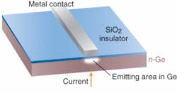
Liu’s group, meanwhile, has been developing a metal-insulator-semiconductor tunnel diode with a metal contact and a silica insulator layer deposited on an n-type germanium substrate. At the end of 2006 the group reported infrared emission near 1.8 µm from a germanium MIS diode cooled to 65 K; the power was about ten times higher than from a similar silicon device.4
Extending the technique
At IEDM, Liu reported extending the technique to produce stimulated emission between 1.6 and 2.2 µm from a Fabry-Perot diode operated at room temperature. The emission comes from a zone in the germanium, just below the insulator and peaked above two microwatts (see Fig. 1). His evidence for lasing includes a rapid increase in efficiency above threshold, strongly directional emission, and line-narrowing above threshold.
However, the news wasn’t all good. Although spontaneous emission from the LED was stable, stimulated emission from the laser spiked sharply at intervals of several seconds although the drive current was steady. Liu suspects carrier trapping and detrapping cycles contribute to the spiking because they’re on the same time scale. And in his prepared abstract he admits, “the laser physics is not well understood.”
Liu says his next step is to grow devices on silicon. “Due to [low] efficiency, an optical interconnect is not practical now,” he says, but that may change. “We have some ideas to improve the efficiency,” he adds.
REFERENCES
1. A.W. Fang, Optics Express 14, 9203 (Oct. 2, 2006).
2. D. Ahn et al., Optics Express 15, 3916 (April 2, 2007).
3. J. Liu et al., Optics Express 15, 11272 (Sept. 3, 2007).
4. M.H. Liao et al., Appl. Phys. Lett. 89, 261913 (2007).
About the Author
Jeff Hecht
Contributing Editor
Jeff Hecht is a regular contributing editor to Laser Focus World and has been covering the laser industry for 35 years. A prolific book author, Jeff's published works include “Understanding Fiber Optics,” “Understanding Lasers,” “The Laser Guidebook,” and “Beam Weapons: The Next Arms Race.” He also has written books on the histories of lasers and fiber optics, including “City of Light: The Story of Fiber Optics,” and “Beam: The Race to Make the Laser.” Find out more at jeffhecht.com.

