NEXT-GENERATION DETECTORS: Plasmon grating-gate devices have potential as tunable terahertz detectors
ERIC A. SHANER, ALBERT D. GRINE, JOHN L. RENO, MIKE C. WANKE, AND S. JAMES ALLEN
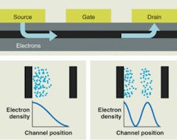
The field-effect transistor (FET) is the cornerstone of modern technological advances such as computer processors and cellular phones. This semiconductor device consists of a “gate” that controls a current flowing through a “channel” using an electric field (see Fig. 1, top). Usually, applications require smaller and smaller FETs (below 100 nm in computer processors running at gigahertz clock frequencies). However, relatively large micron-scale FETs show promise as ultrafast, tunable, narrowband, terahertz photodetectors.1 The key to these FET-based terahertz detectors, such as the grating-gate detector, is that they use collective electron waves called plasmons instead of direct currents.
A semiconductor-based FET is composed of a channel of carriers (electrons or holes), electrical contacts to the channel (commonly called the source and drain), and a gate to control the density of carriers in the channel. In general, the gate/channel part of the device is like a capacitor: changing the voltage on the gate adds or removes charge in the channel. This electrical gate control over the channel enables an FET to function as a switch or amplifier. Plasmons are spatial oscillations of this channel-charge density. Generally, the higher the channel-charge density, the higher the frequency of plasmon oscillations.
Plasmons are poorly matched to the corresponding frequency and wavelength of terahertz radiation. Typical FET carrier densities give rise to plasmon resonances in the terahertz frequency range and wavelengths on the order of microns, whereas terahertz electromagnetic wavelengths measure several hundred microns. Plasmon-based devices therefore require special features, such as antennas or periodic boundaries, to facilitate coupling to the electromagnetic field.
The grating-gate detector is just such a device, combining the charge-density control of a standard FET with the spatial-modulation control of the channel to permit coupling of long-wavelength terahertz radiation to the plasmons. The grating area of these devices is typically on the order of several millimeters, much larger than a normal FET, to match diffraction-limited terahertz beam-spot sizes (see Fig. 2).2 While the devices we study are currently based on high-quality aluminum gallium arsenide/gallium arsenide quantum wells, we expect that grating-gate detectors can be made in any material system that supports FET fabrication (such as silicon).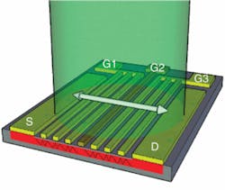
Capabilities
While the grating period sets the plasmon wavelengths in grating-gate detectors, the gate voltage determines the frequency of the plasmon resonances. Current state-of-the-art grating-gate detectors have a special gate line in the center of the device (see Fig. 2).3 Enhanced sensitivity results from biasing this central gate differently than the other gate lines, essentially creating a bolometer (temperature-dependent element) in the FET channel. Grating-gate detectors are polarization dependent and only exhibit a photoresponse when the incident electric field is directed across the grating.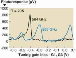
The photoresponse of a grating-gate detector having a 4 µm grating period was measured at 584 and 993 GHz (see Fig. 3). The detector used in the measurements is a depletion-mode device—as the gate bias is made more negative, the number of carriers in the channel is reduced. The single gate line, G2, controls the detector sensitivity and is biased here to a point that produces a large photoresponse. As the gate bias on the tuning gates (G1, G3) is changed, the carrier density in the channel underneath the respective grating gate lines is altered. For a given frequency, sweeping the tuning-gate bias eventually brings a plasmon mode into resonance with the external field. When this occurs, a peak is seen in the photoresponse. Different peaks for a given terahertz excitation correspond to different plasmon standing waves (see Fig. 1, bottom).
Each frequency produces a distinct signature as we sweep the gate bias. This signature opens the possibility for an on-chip terahertz spectrometer with no moving parts. To date, we have measured resonant linewidths below 15 GHz. Once a detector is properly calibrated, rapid spectroscopic analysis is possible (see Fig. 4). Here, we connected the tuning gates to a triangle wave-function generator, and the source/drain connections to an oscilloscope. In this particular device, the voltage ramp generates several plasmon resonances corresponding to a spectral sweep of several hundred GHz in 12.5 ms. The illumination frequency of 694 GHz produced two distinct photoresponse peaks corresponding to different plasmon harmonics. In practice, the multipeak harmonic signatures could be used as a basis for frequency identification. As the two different horizontal axes illustrate, focusing on a particular plasmon mode achieves the spectrometer functionality.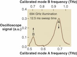
While the devices extensively studied operate from 500 GHz to 1 THz, different grating periods enable access to other frequency ranges. For example, gratings with a 16 µm grating period are useful in the study of direct detection and heterodyne operation at 140 GHz.4 In principle, submicron grating periods could enable higher frequency operation. Furthermore, grating-gate detectors operate at normal incidence with negligible angular dependence, making them suitable for spectroscopic imaging applications.
Outlook
Common semiconductor-based photon detectors rely on excitation of an electron across a bandgap and the release of a photon. This approach fails at terahertz frequencies as the required bandgaps are too small. An appealing characteristic of plasmonic devices is that the underlying resonances do not depend on a bandgap, but instead are related to the motion of charge carriers in an engineered channel. The promise of plasmon-based detectors is best illustrated by comparing it to current technology. Schottky diodes are proven room-temperature microwave detectors; heroic efforts have made them available at terahertz frequencies. Spectroscopic performance in Schottky diodes is achieved in a heterodyne mode that requires a terahertz source to act as a local oscillator (as opposed to the direct detection in grating-gate detectors). A myriad of bolometric detectors, including pyroelectric sensors, Golay cells, and cryogenic bolometers, present the user with interesting and important tradeoffs between operating temperature, sensitivity, and noise-equivalent input power. None can be spectroscopically tuned. Provided adequate sensitivity, the terahertz plasmonic detector offers on-chip spectroscopy in a detector that can be readily integrated into a focal-plane array. Spectroscopic focal-plane arrays can be valuable tools in the terahertz spectral range.
While the key beneficial feature of grating-gate detectors has been identified and documented—a spectrally narrow and tunable terahertz response—the primary focus now is on improved sensitivity and operating temperature to enable imaging applications. To improve sensitivity, we are currently investigating ways to increase radiation absorption in the FET channel and exploring alternative geometries and detection mechanisms to convert the absorbed radiation into electrical signals. Plasmon resonant linewidths will remain narrow up to 100 K, but detection mechanisms invariably lead to reduced sensitivity at elevated temperatures. Researchers are currently pursuing monolithic integration of bolometric and rectifying elements. Many design parameters are available; a design that optimizes material and material structure may potentially pay off in a terahertz spectroscopic imaging system for applications including homeland security, environmental sensing, manufacturing inspection, and combustion engineering in solid fuel rockets.
ACKNOWLEDGMENTS
Sandia is a multiprogram laboratory operated by Sandia Corp., a Lockheed Martin Company, for the U.S. Department of Energy’s National Nuclear Security Administration under contract DE-AC04-94AL85000. Work at UCSB was supported by an ARO-DURINT – The Science and Technology of Nano/Molecular Electronics: Theory, Simulation and Experiment and continues under the University at Buffalo NSF NIRT THz Collaboratory: ECS0609146.
REFERENCES
1. A. El Fatimy et al., Electron. Lett. 42, 1342 (2006).
2. E. Shaner et al., Appl.Phys. Lett. 87, 193507 (2005).
3. E. Shaner et al., IEEE Phot. Tech. Lett. 18, 1925 (2006).
4.Mark Lee et al., Appl. Phys. Lett. 86, 033501 (2005).
Eric A. Shaner is a senior member of technical staff, Albert D. Grine is photonics technician, John L. Reno is principal member of technical staff, and Mike C. Wanke is principal member of technical staff at Sandia National Laboratories, P.O. Box 5800, MS 0316, Albuquerque, NM 87185; e-mail: [email protected]; www.sandia.gov. S. James Allen is professor of physics at the University of California-Santa Barbara, Center for Terahertz Science & Technology, Santa Barbara, CA 93106.