CMOS DETECTORS: Thin-film TECs give new life to CMOS cooling
PAUL MAGILL
Active cooling is becoming essential for many advanced electronic and optoelectronic devices. Two attributes are important for active cooling of components: the ability to maintain a temperature difference between two surfaces and the ability to move heat from one surface to another. For many applications, thermoelectric coolers (TECs)-which are solid-state heat pumps with no moving parts-offer the best solution. Their reliability and ruggedness make them ideal for cooling devices that can be sensitive to mechanical vibration. Their size makes them well suited for applications that are space or weight limited.
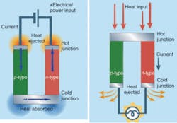
The p-n semiconductor junction in a thermoelectric device can be used either as a TEC based on the Peltier effect or as a thermoelectric generator based on the Seebeck effect (see Fig. 1). In a thermoelectric device used as a TEC, an electric current is driven through a circuit containing two dissimilar materials, heat is absorbed at one junction (the cold side) and released at the other junction (the hot side).
Ideally, the p-n junction is fabricated with materials that have high electrical conductivity and poor thermal conductivity to maximize current flow and minimize heat flowing back from the hot side to the cold side. Because heat naturally flows down a temperature gradient (from hot to cold), the ability of a TEC to move heat from cold to hot in a solid-state fashion is unique. By reversing the polarity of the applied direct current, heating is also possible (the Seebeck effect). This property is especially useful for applications requiring both cooling and heating for precise temperature control of, for example, laser diodes.
The coefficient of performance (COP) is the amount of heat pumping that occurs divided by the amount of supplied electrical power. It is possible, in special situations, for a TEC to pump more watts of heat than the watts of electrical power input it consumes. The COP depends on the application, amount of heat pumped, and temperature differential required. The COP is usually between 0.4 and 0.7 for single-stage applications with a maximum temperature difference (ΔT) on the order of 70°C. It is possible to achieve a higher ΔT by stacking these devices one on the other, but the COP of the combined device then degrades, as heat must now be pumped through an additional module.
Thermoelectric coolers have traditionally been fabricated using bulk materials-processing techniques. Thermoelectric pellets with typical lateral dimensions of 1 × 1 mm and a thickness of 1 mm are assembled into a large array of elements between two ceramic substrates. State-of-the art bulk thermoelectrics can be made with units as thin as 200 µm.
Thin-film TECs
A relatively new development is the manufacture of thin-film TECs, in which semiconductor-processing techniques are used to create a nanostructured film for the p and n portions of the TEC. This technology has been demonstrated at both Nextreme and Research Triangle Institute (Research Triangle Park, NC).
These thin-film TECs have active regions that are typically only 5 to 20 µm thick, resulting in several differences from traditional bulk TECs. First, the heat flux, which is inversely proportional to the thickness of the thermoelectric material. A typical device pumps a maximum heat flux of 150 W/cm2 with some designs delivering as much as 400 W/cm2 versus 10 to 20 W/cm2 for typical bulk TECs. Second, thin-film TECs can operate in a high-COP regime and still pump a reasonably high heat flux (50 to 100 W/cm2). And finally, while bulk TECs have response times on the order of seconds, thin-film TECs have a very fast millisecond response time, allowing rapid cooling and heating adjustments to maintain a precise temperature.
Thermoelectric coolers are generally defined by what is called their load line, which is the ΔT produced at a fixed, specified operating current and temperature. The two environmental parameters that a TEC can alter are the temperature and the heat content of the device to be cooled; a TEC will tend to operate such that it optimizes one or the other. Standard TECs typically have the capability to produce a large ΔT between two objects but cannot pump much heat; thus, they will work well for objects that have very low heat content. The thin-film TEC, on the other hand, can pump a lot of heat but maintains a smaller ΔT-in part because it is much thinner. This gap between maximum ΔT of bulk and thin film TECs is rapidly closing. In fact, thin-film TECs have recently been measured to have a ΔT 60 K.
Cooling of CMOS devices
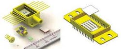
The thin-film TEC form is quite adaptable and can be used in many types of optoelectronic packages, including those for laser diodes, CMOS sensors and other imagers, and photodetectors. The implementation of a thin-film TEC for a typical CMOS imaging sensor can consist of an array of individual TEC components (see Fig. 2). The detailed geometry would depend on how and where the heat is generated.The largest contributor to the noise component of a CMOS optical sensor is what is termed the dark current (resulting from shot and Johnson noise), and is defined as the external current that, under specified biasing conditions, flows in a photoconductive detector when there is no incident radiation. This in turn is a function of the temperature to which the device is cooled.
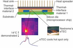
Cooling of a CMOS detector generally requires lowering of the temperature across the entire active region, requiring that the thermocouples be evenly spread across the device. However, densely populating the region with thermocouples is not always necessary and has the possible disadvantage of greater power consumption. Alternatively, a thin-film TEC can be designed to cool hot spots (see Fig. 3).The detailed characteristics of the thin-film TEC depend on the application. If power consumption is not a concern, obtaining the largest ΔT across the TEC film would be the likely goal. If power consumption is an important consideration, as for instance in a battery-powered CMOS-detector-based instrument, then a trade-off analysis should be done to determine the optimal balance between CMOS signal-to-noise ratio and battery life/power consumption (the lower the ΔT, the lower the power consumption).
Apart from the two TE characteristics of ΔT and Qmax (heat-pumping capacity in watts), the COP is also a factor to consider in designing cooling for CMOS devices. A higher COP means that less power must be used to move one unit of heat; this results in a device that consumes a fraction of the total power of a device with a lower COP. This parameter is extremely important in the use of battery-powered IR imagers, as the amount of power required for additional cooling increases significantly with increased ΔT. A COP reduced in this way can fall below 0.25 for a large enough ΔT-meaning that, for instance, four watts of input power must be supplied for every watt of cooling that results.
Wider use of thin-film TECs
Thermal-management concerns exist across the board and in a broad spectrum of photonic devices, not just CMOS sensors. These concerns range from the need to produce a large temperature reduction in solid-state sensors, to the need to pump large amounts of heat from high-power laser diodes. In addition, the drive to cheaper and smaller packaging is forcing the thermal-design engineer to consider alternative implementations of TEC technology.
Thermoelectric devices are used industry-wide as a means of solving difficult thermal-management problems. The thermal-management industry now offers both a traditional TEC, with its larger ΔT, and a new thin-film version, which offers the promise of a solution for some of the most critical and intractable thermal issues.
PAUL MAGILL is vice president of marketing and business development for Nextreme, 3040 Cornwallis Rd., Research Triangle Park, NC 27709; e-mail: [email protected]; www.nextreme.com.


