SEMICONDUCTOR DETECTORS: Germanium on silicon approaches III-V semiconductors in performance
MIKE MORSE
Silicon photonics has been getting increased attention in the press as companies and universities report on advances that appear to be opening the door for widespread use of this technology in optical communications. While there is still some uncertainty about what the first high-volume application might be, developing the fundamental components is a necessary first step toward commercializing the technology. At Intel, research has been focused on demonstrating these building blocks, which include modulators, hybrid lasers, and photodetectors, together with passive waveguides to tie the devices together. While the press has devoted less attention to the photodetectors than the other components (the lasers in particular), advances in germanium-on-silicon (Ge/Si) photodiodes are proceeding apace (see Fig. 1).
Materials issues for detectors
Silicon itself has been shown to be an excellent photodetector material with a quantum efficiency of virtually 100%. Unfortunately, the useful wavelength range for Si falls in the visible spectrum, rather than the near-IR spectral region of 1.31 to 1.55 µm typically used for communications (see Fig. 2). Even though some absorption occurs in Si up to the indirect band edge (1.1 µm), the penetration depth of the light at longer wavelengths is too long to effectively and quickly capture the photocarriers created by it.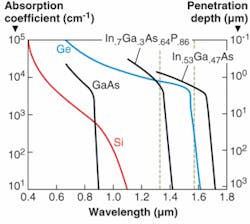
Germanium has a much higher absorption coefficient in the wavelength range of interest. Most leading integrated-circuit producers already use Ge in the chip-making process to improve transistor performance (by creating strained Si); thus, Ge is relatively easy to introduce to enhance optical performance as well. Unstrained, pure Ge can detect light up to 1.6 µm, albeit with a low absorption coefficient. Adding strain to the material has been shown to push the band edge out to longer wavelengths and increase the absorption coefficient significantly at the important 1.55 µm wavelength.
While some strain is beneficial for longer-wavelength detection, too much is not a good thing. In fact, the most serious drawback to using Ge on Si for photodetection is the strain caused by the 4% lattice mismatch. This mismatch can drive the introduction of dislocations that harm device performance. This is contrary to the situation for III-V semiconductors, in which ternary materials can be used to lattice-match to the substrate (for example, gallium arsenide (GaAs) or indium phosphide (InP), giving the designer tremendous flexibility for device optimization. Some research in Ge/Si photodetectors has focused on using multiple quantum wells or even Ge quantum dots to avoid the introduction of dislocations caused by the relaxation of the Ge films as the critical thickness is exceeded. Most work, however, accepts the formation of misfit and threading dislocations during the growth of thick Ge films with the belief that later processing can reduce their impact. The most common approach to doing this is to carry out an annealing step, after which the threading-dislocation density can be reduced to on the order of 106 dislocations/cm2—which is still two to three orders of magnitude higher than that found in lattice-matched III-V heterostructures.
Detector structure and performance
Given the range of spectral absorption coefficients and the desire to develop products that operate between 0.85 to 1.55 µm, two different types of germanium-based structures are commonly discussed. At the low end of the range (0.85 to about 1.3 µm), the absorption coefficient of germanium is high enough to support high responsivity and bandwidth with films only a few microns thick. This allows for the use of a vertical p-i-n device that is typical for GaAs and InP devices in the market today. These devices are illuminated from the top or bottom.
At wavelengths approaching 1.55 μm, however, the thickness of Ge needed to absorb enough of the light precludes fast device performance in a vertical p-i-n structure. As a result, waveguide-based detectors are considered more promising because they decouple the absorption depth of the light from the photocarrier transit time, which is normally perpendicular to the waveguide direction. This means that high responsivity and bandwidth are possible. The additional benefit of moving into a waveguide device is that it brings the possibility of integration with other optical devices, the result of which could enable very densely packed, high-bandwidth transceivers.
Three critical performance metrics for any photodetector are responsivity, dark current, and bandwidth. Normal device specifications for these parameters in commercial III-V 10 Gbit/s photodetectors are 0.6 to 0.9 A/W (at 0.85 to 1.55 μm wavelengths), 1 nA, and greater than 8 GHz, respectively at a few volts bias. Intel researchers have demonstrated Ge vertical p-i-n detectors with a form factor comparable to commercial GaAs devices that have been able to match two of these metrics. For 50-µm-diameter detectors with a 1.5-µm-thick Ge film on Si, a responsivity of 0.65 A/W and a bandwidth of 9 GHz have been measured at a wavelength of 0.85 µm. The dark current at a 2 V reverse bias is about 150 nA and is dominated by an area-dependent factor, most likely caused by the threading dislocation density. While this is much higher than that of a GaAs device, it still is lower than the input-referred noise current of a typical transimpedance amplifier used in receivers.
The consequence is that the overall noise in a receiver is not impacted by the relatively noisy Ge photodetector. In fact, for two receivers that are identical except that one has a Ge detector and the other a GaAs detector, the resulting 10 Gbit/s eye diagrams are virtually indistinguishable.
Even more critical is the measurement of sensitivity as a function of temperature. One initial concern was that, even when a receiver based on a Ge detector is within specification at room temperature, the detector dark current might increase so quickly as the temperature is raised that it would become larger than the amplifier noise. A sensitivity test was performed on receivers based on Ge and GaAs detectors from -20°C to 85°C; both receivers were within the sensitivity specification over the entire operational range (see Fig. 3). The receiver with the Ge detector had a 1 dB penalty in this test due to reduced optical coupling into a smaller Ge detector (50 µm diameter) compared to the GaAs detector (75 µm diameter).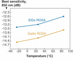
Research on waveguide-based devices is also well under way in a number of places. The majority of the effort centers on using waveguides made from silicon on insulator (SOI) wafers. The silicon waveguide is formed by etching a rib or strip in the top silicon layer located above an oxide layer. Germanium can be grown on top of the waveguide or at the end of the waveguide to get efficient coupling.
Drive for commercialization
With the performance of receivers based on Ge photodetectors approaching or equal to the desired optical and electrical specifications, the remaining items to be addressed are reliability and cost. The large number of dislocations does give rise to concerns about passing qualification standards (Telcordia GR-468 CORE). Devices made at Intel are currently undergoing preliminary tests with positive results to date. A high-temperature-storage test done at 170°C for one month did not cause any degradation in dark current or responsivity. More important, virtually all devices subjected to a reverse bias of 6 V and 200°C of stress for nearly 900 hours showed very little increase in dark current and no responsivity change caused by device degradation.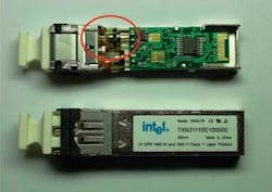
Intel is currently exploring the use of normal-incidence and waveguide photodetectors for commercialization. For example, a 4 Gbit/s transceiver has been made with a germanium photodetector that serves as a drop-in replacement for a GaAs detector (see Fig. 4). Learning from these types of modules in existing high-volume applications can allow for further advances in performance and, more important, the acceptance of the more-complicated integrated parts to be developed. With the rapid rate of improvement that has been seen in these detectors, it is likely that only the marketplace will determine how successful they are.
Mike Morse is senior silicon-photonics researcher at Intel Corp., 2200 Mission College Blvd., Santa Clara, CA 95052; e-mail: [email protected]; www.intel.com.