SILICON PHOTONICS: Silicon-waveguide modulator reaches 30 Gbit/s
Aiming to create all the building blocks needed for a complete high-speed silicon-photonics data-transmission system, researchers at Intel (Santa Clara, CA) have unveiled a silicon-based optical modulator that operates at 30 Gbit/s. Combined with the hybrid laser already announced by Intel (see “Conference Preview: Photonics West 2007,” www.laserfocusworld.com/articles/279850), the devices will form a high-data-rate light source; other components of the system will include an optical-fiber link and a silicon photodetector (also being developed at Intel).
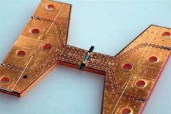
The optical modulator, which contains two p-n junctions, each in a silicon-on-insulator waveguide that is an arm of a Mach-Zehnder interferometer, is based on the free-carrier plasma-dispersion effect, in which the refractive index changes as a function of electric-field-induced carrier depletion. Optimum electronic performance is crucial; the device is designed so that the electrical and optical signals propagate together down the waveguide. The device can be modulated at 20 GHz (3 dB bandwidth).
Intel aims to boost the data rate further to 40 Gbit/s, and to integrate dozens of modulators onto a single chip that will also include hybrid lasers of different wavelengths and a multiplexer to combine their signals; 25 laser/modulators on a chip would result in a terabit transmission capability, all integrated in silicon (except for the optical fiber). In one potential use, many boards containing these silicon-photonic chips would coexist side by side, communicating with each other to form a supercomputer far beyond the scale of today’s fastest computer. The chips will also be well suited for use in general data communications and computing.
Phase-modulation efficiency was improved by reducing the waveguides to submicrometer dimensions, with widths of 0.6 µm, rib heights of 0.5 µm, and an etch depth of 0.2 µm. A multimode-interference coupler was used to split the incoming signal, as such a coupler has a larger spectral bandwidth and larger fabrication tolerances than a directional coupler. The on-chip insertion loss of the modulator in its transmissive state is about 7 dB; most of this (5.4 dB) is due to the dopants in the phase-shifter (modeling shows that improvements can reduce the phase-shifter loss to 2 dB).
Asymmetric contact design
The waveguides were combined with a coplanar traveling-wave electrode design, which minimizes the so-called RC dependence (a lag arising from resistive and capacitive effects) to permit highest speed performance. “The asymmetric contact design of the electrodes allows for optimum electrical performance while minimizing the optical loss,” notes Mario Paniccia, director of the Photonics Technology Lab at Intel.
The fact that this technology resides at Intel will certainly not hinder its integration into computer chips. “As we scale future microprocessors to many, if not hundreds, of cores, we will need to route terabits of information in and around the processors,” says Paniccia. “We now have all the silicon-photonics devices available in our toolbox and can now start to integrate these building blocks together. One can now see a path to integrating silicon hybrid lasers, photodetectors, modulators, and waveguides into a single highly integrated photonic chip capable of transmitting 1 Tbit/s of information down a single optical fiber all on a piece of silicon the size of your fingernail.”
Intel will continue to improve the speed, reduce the size, and reduce the power consumption of the modulator, adds Paniccia. “The next steps are to continue to optimize the electrical termination of the current design and demonstrate performance at 40 Gbit/s,” he says. “In addition, we will continue to improve the device to operate at lower operating voltage and have better phase efficiency, and will incorporate tapers to improve the the fiber-coupling efficiency.”
REFERENCE
1. A. Liu et al., Optics Express 15(2) (January 2007).
About the Author

John Wallace
Senior Technical Editor (1998-2022)
John Wallace was with Laser Focus World for nearly 25 years, retiring in late June 2022. He obtained a bachelor's degree in mechanical engineering and physics at Rutgers University and a master's in optical engineering at the University of Rochester. Before becoming an editor, John worked as an engineer at RCA, Exxon, Eastman Kodak, and GCA Corporation.