OPTICAL TRAPPING: Optical waveguides and microfluidics join forces in novel lab-on-a-chip design
Researchers at Cornell University (Ithaca, NY) have for the first time integrated planar waveguides with microfluidic channels on a miniaturized optical-trapping platform that could find application in telecom, datacom, and the life sciences.1
According to Michal Lipson, assistant professor of electrical and computer engineering at Cornell and lead researcher on this project, the waveguides used in the device achieve a more-efficient sorting process that enables the manipulation of smaller spheres at lower laser intensities than previously reported. By integrating these waveguides with microfluidic channels created via conventional soft-lithography techniques, Lipson and her colleagues have developed a simple, portable sorting system that allows them to control the movement of particles in a pressure-driven flow, resulting in hundreds of measurements in parallel on a 1 × 1 cm chip with greater efficiency and at lower cost than is possible with current trapping and sorting methods.
The Cornell optofluidics system features polydimethylsiloxane (PDMS) microfluidic channels fabricated on a fused-silica substrate using standard soft-lithography techniques, and solid-core planar waveguides built into the walls of each microfluidic channel. The waveguides were fabricated using SU-8, a common negative polymer photoresist that can be spun or spread over thicknesses from 1 µm to 2 mm and still be processed via standard photomask processes. It is mainly used in the fabrication of microfluidics and MEMS parts and is an extremely bio-compatible material.
The light source in the experiments was a fiber-coupled laser-diode module (975 nm) connected to an isolator to protect the laser from back reflections. A polarization controller was used to measure the input power that was then coupled to a lensed fiber. The lensed fiber coupled light into the waveguides, and the output light was collected with an objective lens and measured with a standard photodetector. The PDMS fluidic layer was bonded 600 µm from the edge of the chip to allow clear imaging of the fiber-to-waveguide alignment and to ensure that the single-mode air-clad structure would prevent the excitation of second-order modes. The particles used in the experiment were polystyrene spheres of various sizes at a concentration of 0.1 to 0.2 g/L in a 100 mM phosphate buffer solution with a regulated pH of 7.0.
“The planar optofluidic architecture represents a simple yet functional optical manipulation system for lab-on-chip applications,” Lipson said. “Such a system could find application in high-stability particle trapping and sorting, and also for biomolecular detection by exploiting the strong light scattering observed when a particle interacts with the evanescent field.”
Evanescent field
In fact, the evanescent field is a key factor in the success of the Cornell lab-on-a-chip. According to Lipson, previous experiments using evanescent fields for optical trapping have shown that these fields are responsible for propulsion of dielectric particles along waveguides made of ion-exchange doped glasses and silicon nitride waveguides within static fluid cells. Lipson and her colleagues decided to extend this research to demonstrate how the evanescent field surrounding a solid-core planar waveguide can directly capture and transport dielectric particles initially carried within a pressure-driven flow. They also wanted to capture and transport particles both perpendicular and opposite to an imposed pressure-driven flow along both straights and curved waveguides.
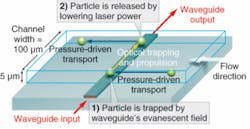
“The forces exerted by the evanescent field in the waveguides resulted in both the attraction of particles to the waveguide surface and propulsion in the direction of optical propagation both perpendicular and opposite to the direction of pressure-driven flow,” Lipson said (see figure). Velocities as high as 28 µm/s were achieved for 3-µm-diameter polystyrene spheres with an estimated 53.5 mW of guided optical power at the trapping location.
REFERENCE
Optics Express 15(22) 14322 (Oct. 29, 2007).
About the Author
Kathy Kincade
Contributing Editor
Kathy Kincade is the founding editor of BioOptics World and a veteran reporter on optical technologies for biomedicine. She also served as the editor-in-chief of DrBicuspid.com, a web portal for dental professionals.
