NANOPHOTONICS: Tiniest lasers aim for the optical-computing frontier

One of the major stumbling blocks for the oft-touted “optical computer” is simple: size. The continuing expansion in the fiber-optic telecommunications industry has made a niche for microscale lasers, and these advances have kept open the possibility of optical computing. Systems of lasers can in principle perform as digital switching networks, with potentially higher performance than their semiconductor counterparts—if only they could slim down. Optical fibers offer lots of bandwidth but are bulkier than simple wires. Optical sources have to compete with the semiconductor industry’s ever-shrinking transistor dimensions.
A promising new approach is at hand. Research by collaborators in the Netherlands and Korea has demonstrated the smallest electrically pumped lasers ever.1 The devices are metal-encapsulated nanocavities as small as 210 nm across that support low-power, high-Q lasing. The work is not just a single step down in size; the researchers claim that the process lends itself to resonators another order of magnitude smaller.
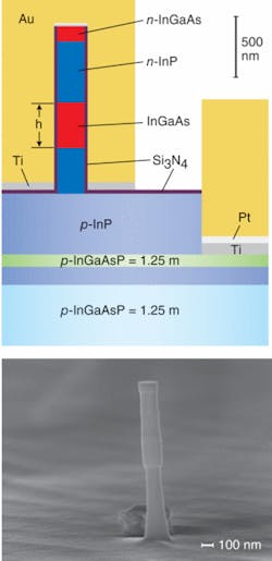
At the core of the devices is an epitaxially grown indium phosphide/indium gallium arsenide/indium phosphide pillar of about 300 nm height and varying diameter. It is surrounded by a 10 nm silicon nitride insulating layer fabricated by chemical-vapor deposition. The whole heterostructure is encapsulated in gold, forming a metallic cavity (see figure).
A small amount of the mode energy escapes through the bottom of the pillar, allowing the researchers to have a peek at what is happening inside the cavity (future applications may couple the energy out via metallic waveguides). They found that the heterostructure had well-confined modes resonant at a wavelength of 1408 nm and a linewidth of 0.3 nm. The cavity Q was just 48 at room temperature, and was dominated by optical losses in the gold-a result that has held back previous metallic-cavity nanolasers. However, that value increases at low temperature; the team measured Q values of 140 and 200 at temperatures of 77 and 10 K, respectively.
Possible use in plasmonics
But this story of the small gets better. “This is only the start of the miniaturization process,” says Martin Hill of the COBRA Research Institute (Eindhoven, The Netherlands) and lead author of the study. Finite-difference-time-domain simulations show that the devices can be made to cross an even more important size gap-that between photonics and plasmonics, the interaction of light with surface plasmons. The lure of this kind of subwavelength optical processing has formed speculation about the future of computing for years.
“Initially I thought of making the devices more as an interesting scientific exercise. However, in the beginning of 2007, I had the chance to sit back a bit and see how it fit into plasmonics,” Hill says. “The same structure and construction techniques can be used to make cavities that have a surface-plasmon-polariton gap mode.”
The key to that development is in varying the shape and dimensions of the pillar. “The plasmon-gap-mode waveguides provide the framework to do all sorts of complex things in VLSI (very-large-scale-integrated) photonic devices,” Hill says. “But the structure of the diode encapsulated in metal with lithographically defined cross section, and mode in the middle of the pillar defined by the wafer epitaxy, will form the basis for all this.” The researchers compared two devices with pillar diameters differing by 30 nm; their lasing wavelength was different by some 144 nm. By using a rectangular cross section, simulations predict that cavity size can be reduced to just a few tens of nanometers in height and in one lateral dimension.
The result is important because of the limitations imposed by optical losses in plasmonic systems. “In current subwavelength plasmonic systems, the signals are attenuated quickly, but with the active structures we show the loss could be overcome, allowing complex subwavelength optical systems to be made.” That means devices down to sizes of just tens of nanometers or less, with active, subwavelength waveguides that connect the tiny lasers.
Amnon Yariv of the California Institute of Technology (Pasadena, CA), is another past master of tiny indium-based lasers.2 He describes the recent research as a “hero experiment,” but warns that the metallic encapsulation leads to broad linewidths and reduced coherence. Hill’s researchers are convinced that their proof-of-principle demonstration is ripe for improvement, analogous to the situation for early bandgap-defect and microdisk lasers. The team is, for the moment, replacing the gold encapsulation layer with silver, an improvement that simulations predict will increase the room-temperature cavity Q to higher than that demonstrated at 77 K in the research.
REFERENCES
1. M.T. Hill et. al., Nature Photonics1, 589 (October 2007).
2. J. Scheuer, et. al., Appl. Phys. Lett.60, 289 (2005).